Images are for reference only See Product Specifications
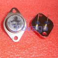
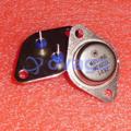
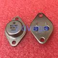
2N4117A
TO-72 packaged N-type junction field-effect transistor (JFET)


RoHS Status:
Stock Condition: 5827 pcs, New Original
Warranty: 1 Year Ovaga Warranty - Find Out More
0
1
Add To Bom2N4117A General Description
2N4117A is a JFET (junction field-effect transistor) semiconductor device that is commonly used in low-power amplifier and switching applications. It is a small signal N-channel JFET with a TO-18 package.The key specifications of the 2N4117A are as follows:1. Maximum Drain-Source Voltage (Vds): 35V2. Maximum Gate-Source Voltage (Vgs): -35V3. Maximum Drain Current (Id): 10mA4. Maximum Power Dissipation (Pd): 350mW5. Input Capacitance (Ciss): 6pF6. Gate-Source Cutoff Voltage (Vgs(off)): -1V to -8V7. Forward Transfer Admittance (Yfs): 1.5mA/VThe 2N4117A offers low noise, high input impedance, and good gain characteristics, making it suitable for applications where these properties are important. It is commonly used in audio amplifiers, instrumentation, and other low-power signal processing circuits.It is important to note that JFETs like the 2N4117A are voltage-controlled devices, where the input signal is applied to the gate terminal to control the current flow between the drain and source terminals. Care must be taken to handle and bias the JFET correctly to ensure proper operation and performance in a circuit.
Features
- P-channel JFET transistor
- Low noise, high gain
- Designed for audio applications
- High input impedance
- Low distortion
- Excellent high-frequency response
- Can be used in amplifiers, preamplifiers, and buffering circuits
- TO-18 metal can package
- Operating temperature range: -55°C to 125°C
Application
- Low frequency amplification
- Switching applications
- Signal processing
- Audio amplification
- Instrumentation
- Test equipment
- Communications systems
- Measurement systems
- Frequency generators
- Audio mixers
Specifications
| Parameter | Value | Parameter | Value |
|---|---|---|---|
| Product Category | JFET | RoHS | Details |
| Technology | Si | Mounting Style | Through Hole |
| Package / Case | TO-72-4 | Transistor Polarity | N-Channel |
| Configuration | Single | Vds - Drain-Source Breakdown Voltage | 10 V |
| Vgs - Gate-Source Breakdown Voltage | - 40 V | Gate-Source Cutoff Voltage | - 1.8 V |
| Drain-Source Current at Vgs=0 | 90 uA | Id - Continuous Drain Current | 1 nA |
| Pd - Power Dissipation | 300 mW | Series | 2N411 |
| Brand | InterFET | Forward Transconductance - Min | 70 uS |
| Product Type | JFETs | Factory Pack Quantity | 1 |
| Subcategory | Transistors | Type | JFET |
| Unit Weight | 0.023558 oz |
Shipping
| Shipping Type | Ship Fee | Lead Time | |
|---|---|---|---|
 |
DHL | $20.00-$40.00 (0.50 KG) | 2-5 days |
 |
Fedex | $20.00-$40.00 (0.50 KG) | 2-5 days |
 |
UPS | $20.00-$40.00 (0.50 KG) | 2-5 days |
 |
TNT | $20.00-$40.00 (0.50 KG) | 2-5 days |
 |
EMS | $20.00-$40.00 (0.50 KG) | 2-5 days |
 |
REGISTERED AIR MAIL | $20.00-$40.00 (0.50 KG) | 2-5 days |
Processing Time:Shipping fee depend on different zone and country.
Payment
| Terms of payment | Hand Fee | |
|---|---|---|
 |
Wire Transfer | charge US$30.00 banking fee. |
 |
Paypal | charge 4.0% service fee. |
 |
Credit Card | charge 3.5% service fee. |
 |
Western Union | charge US.00 banking fee. |
 |
Money Gram | charge US$0.00 banking fee. |
Guarantees
1.The electronic components you purchase include 365 Days Warranty, We guarantee product quality.
2.If some of the items you received aren't of perfect quality, we would resiponsibly arrange your refund or replacement. But the items must remain their orginal condition.
Packing
-

Step1 :Product
-

Step2 :Vacuum packaging
-

Step3 :Anti-static bag
-

Step4 :Individual packaging
-

Step5 :Packaging boxes
-

Step6 :bar-code shipping tag


All the products will packing in anti-staticbag. Ship with ESD antistatic protection.
Outside ESD packing’s lable will use ourcompany’s information: Part Mumber, Brand and Quantity.
We will inspect all the goods before shipment,ensure all the products at good condition and ensure the parts are new originalmatch datasheet.
After all the goods are ensure no problems afterpacking, we will packing safely and send by global express. It exhibitsexcellent puncture and tear resistance along with good seal integrity.


Part points
-
The 2N4117A is a high-performance JFET transistor commonly used for low power amplifier applications. It has a low noise figure and high input impedance, making it a popular choice for signal amplification in audio circuits and radio frequency applications. Its compact size and reliable performance make it a versatile option for various electronic projects.
-
Equivalent
The equivalent products of 2N4117A chip are J112, 2SK246, MPF102, and NTE451. These transistors are all JFETs with similar specifications and can be used as substitutes for the 2N4117A in various electronic circuits. -
Features
The 2N4117A is a small-signal N-channel JFET with high input impedance, low input capacitance, and low noise figure. It is commonly used in amplifier and switching applications due to its high-frequency performance and low distortion characteristics. -
Pinout
The 2N4117A is a JFET transistor with 3 pins: gate (G), drain (D), and source (S). It is a N-channel JFET and has a pin count of 3. It functions as a voltage-controlled current regulator, used in amplification and switching applications. -
Manufacturer
The 2N4117A is manufactured by ON Semiconductor. ON Semiconductor is a global supplier of power and signal management, discrete, logic, and custom devices for various applications including automotive, communications, industrial, medical, and aerospace. The company focuses on energy-efficient solutions and sustainability in its products and operations. -
Application Field
The 2N4117A is commonly used for applications in low-frequency and low-power analog circuits, such as amplifiers, oscillators, and switches. It can also be utilized in audio amplifiers, signal processing circuits, and sensor interfaces due to its low noise and high gain characteristics. -
Package
The 2N4117A chip is a TO-18 metal can package type with three leads. It is in the form of a discrete semiconductor component. The size of the chip is 2.16mm x 4.70mm x 4.70mm.


We provide high quality products, thoughtful service and after sale guarantee
-

We have rich products, can meet your various needs.
-

Minimum order quantity starts from 1pcs.
-

Lowest international shipping fee starts from $0.00
-

365 days quality guarantee for all products