Images are for reference only See Product Specifications
TI TPS22962DNYR
Power Switch/Driver 1:1 N-Channel 10A 8-WSON (3x3)


Brands: TI
Mfr.Part #: TPS22962DNYR
Datasheet: TPS22962DNYR Datasheet (PDF)
Package/Case: WSON-8
Product Type: Power Distribution Switches, Load Drivers
RoHS Status:
Stock Condition: 19 pcs, New Original
Warranty: 1 Year Ovaga Warranty - Find Out More
0
1
Add To BomTPS22962DNYR General Description
The TPS22962 is a small, ultra-low RON, single channel load switch with controlled turn on. The device contains an N-channel MOSFET that can operate over an input voltage range of 0.8 V to 5.5 V and supports a maximum continuous current of 10 A.
The combination of ultra-low RON and high current capability of the device makes it ideal for driving processor rails with very tight voltage dropout tolerances. The controlled rise time of the device greatly reduces inrush current caused by large bulk load capacitances, thereby reducing or eliminating voltage droop on the power supply. The switch can be independently controlled via the ON pin, which is capable of interfacing directly with low-voltage control signals originating from microcontrollers or low voltage discrete logic. The device further reduces the total solution size by integrating a 224-Ω pull-down resistor for quick output discharge (QOD) when the switch is turned off.
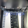
The TPS22962 is available in a small 3.00 mm x 3.00 mm WSON-8 package (DNY). The DNY package integrates a thermal pad which allows for high power dissipation in high current and high temperature applications. The device is characterized for operation over the free-air temperature range of –40°C to 105°C.
Features
- Integrated Single Channel Load Switch
- VBIAS Voltage Range: 2.5 V to 5.5 V
- VIN Voltage Range: 0.8 V to 5.5 V
- Ultra Low RON Resistance
- RON = 4.4 mΩ at VIN = 5 V (VBIAS = 5 V)
- 10 A Maximum Continuous Switch Current
- Low Quiescent Current
- (20 µA for VBIAS = 5 V)
- Low Shutdown Current
- (1 µA for VBIAS = 5 V)
- Low Control Input Threshold Enables Use of 1.2 V or Higher GPIO
- Controlled and Fixed Slew Rate Across VBIAS and VIN
- tR = 2663 µs at VIN = 5 V (VBIAS = 5 V)
- Quick Output Discharge (QOD)
- SON 8-Pin Package with Thermal Pad
- ESD Performance Tested per JESD 22
- 2-kV Human-Body Model (HBM)
- 1-kV Charged-Device Model (CDM)
Specifications
| Parameter | Value | Parameter | Value |
|---|---|---|---|
| Number of channels | 1 | Vin (min) (V) | 0.8 |
| Vin (max) (V) | 5.5 | Imax (A) | 10 |
| Ron (typ) (mΩ) | 4.4 | Shutdown current (ISD) (typ) (µA) | 1.1 |
| Quiescent current (Iq) (typ) (µA) | 20.4 | Soft start | Fixed Rise Time |
| Current limit type | None | Features | Quick output discharge |
| Rating | Catalog | Operating temperature range (°C) | -40 to 85 |
| FET | Internal | Device type | Load switches |
| Function | Inrush current control |
Shipping
| Shipping Type | Ship Fee | Lead Time | |
|---|---|---|---|
 |
DHL | $20.00-$40.00 (0.50 KG) | 2-5 days |
 |
Fedex | $20.00-$40.00 (0.50 KG) | 2-5 days |
 |
UPS | $20.00-$40.00 (0.50 KG) | 2-5 days |
 |
TNT | $20.00-$40.00 (0.50 KG) | 2-5 days |
 |
EMS | $20.00-$40.00 (0.50 KG) | 2-5 days |
 |
REGISTERED AIR MAIL | $20.00-$40.00 (0.50 KG) | 2-5 days |
Processing Time:Shipping fee depend on different zone and country.
Payment
| Terms of payment | Hand Fee | |
|---|---|---|
 |
Wire Transfer | charge US$30.00 banking fee. |
 |
Paypal | charge 4.0% service fee. |
 |
Credit Card | charge 3.5% service fee. |
 |
Western Union | charge US.00 banking fee. |
 |
Money Gram | charge US$0.00 banking fee. |
Guarantees
1.The electronic components you purchase include 365 Days Warranty, We guarantee product quality.
2.If some of the items you received aren't of perfect quality, we would resiponsibly arrange your refund or replacement. But the items must remain their orginal condition.
Packing
-

Step1 :Product
-

Step2 :Vacuum packaging
-

Step3 :Anti-static bag
-

Step4 :Individual packaging
-

Step5 :Packaging boxes
-

Step6 :bar-code shipping tag


All the products will packing in anti-staticbag. Ship with ESD antistatic protection.
Outside ESD packing’s lable will use ourcompany’s information: Part Mumber, Brand and Quantity.
We will inspect all the goods before shipment,ensure all the products at good condition and ensure the parts are new originalmatch datasheet.
After all the goods are ensure no problems afterpacking, we will packing safely and send by global express. It exhibitsexcellent puncture and tear resistance along with good seal integrity.


Part points
-
The TPS22962DNYR chip is a load switch that provides power distribution control. It features a low on-resistance and a wide input voltage range, making it suitable for various applications. Its small package size and high efficiency make it an ideal choice for portable devices and power management systems.
-
Equivalent
Some equivalent products of TPS22962DNYR chip are TPS22963DNYR, TPS22961DNYR, and TPS22960DNYR. These chips are also load switches with similar features and specifications, making them suitable alternatives for various applications. -
Features
The TPS22962DNYR is a load switch with an integrated FET, providing a low on-resistance (17 mΩ typical), a low quiescent current (4.5 µA), and a wide input voltage range (0.5 V to 5.5 V). It also features a thermal shutdown function and is available in a small, space-saving DFN package. -
Pinout
The TPS22962DNYR is a load switch with a pin count of 6. Pin 1 is EN (enable), Pin 2 is GND, Pin 3 is OUT (output), Pin 4 is IN (input), Pin 5 is NC (no connect), and Pin 6 is VIN (input voltage). It controls the power distribution in portable and battery-operated electronics. -
Manufacturer
The TPS22962DNYR is manufactured by Texas Instruments, a multinational semiconductor company that designs and manufactures electronics components, such as integrated circuits and microcontrollers. Texas Instruments is known for its extensive product line in the semiconductor industry, including analog and embedded processors, power management, and educational technology products. -
Application Field
The TPS22962DNYR is commonly used in portable electronic devices, smartphones, tablets, wearables, and other battery-powered systems to control power management functions such as load switching and voltage protection. Additionally, it is also used in power distribution systems, battery chargers, and other applications requiring power sequencing and protection. -
Package
The TPS22962DNYR chip comes in a 4-Son package type. It is a dual-channel load switch with a form of Wafer Level Chip Scale Package (WSON) and a size of 1.5mm x 1.5mm.


We provide high quality products, thoughtful service and after sale guarantee
-

We have rich products, can meet your various needs.
-

Minimum order quantity starts from 1pcs.
-

Lowest international shipping fee starts from $0.00
-

365 days quality guarantee for all products