


Images are for reference only See Product Specifications
TI TLC555QDRQ1
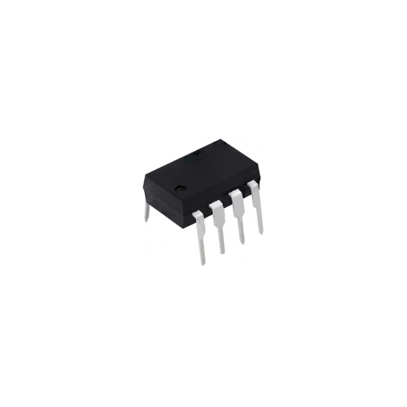
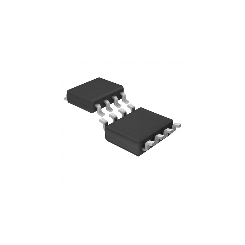
555 Type, Timer/Oscillator (Single) IC 2.1MHz 8-SOIC


RoHS Status:
Stock Condition: 9696 pcs, New Original
Warranty: 1 Year Ovaga Warranty - Find Out More
0
1
Add To BomTLC555QDRQ1 General Description
The TLC555-Q1 is a monolithic timing circuit fabricated using the TI LinCMOS™ process. The timer is fully compatible with CMOS, TTL, and MOS logic and operates at frequencies up to 2 MHz. Because of its high input impedance, this device uses smaller timing capacitors than those used by the NE555. As a result, more accurate time delays and oscillations are possible. Power consumption is low across the full range of power-supply voltage.
Like the NE555, the TLC555-Q1 has a trigger level equal to approximately one-third of the supply voltage and a threshold level equal to approximately two-thirds of the supply voltage. These levels can be altered by use of the control voltage terminal (CONT).
When the trigger input (TRIG) falling below the trigger level sets the flip-flop, and the output goes high. Having TRIG above the trigger level and the threshold input (THRES) above the threshold level resets the flip-flop, and the output is low. The reset input (RESET) can override all other inputs, and a possible use is to initiate a new timing cycle. RESET going low resets the flip-flop, and the output is low. Whenever the output is low, a low-impedance path exists between the discharge terminal (DISCH) and GND. Tie all unused inputs to an appropriate logic level to prevent false triggering.
The advantage of the TLC555-Q1 is that it exhibits greatly reduced supply-current spikes during output transitions. Although the CMOS output is capable of sinking over 100 mA and sourcing over 10 mA, the main reason the TLC555-Q1 is able to have low current spikes is due to its edge rates. This minimizes the need for the large decoupling capacitors required by the NE555.
The TLC555-Q1 is characterized for operation over the full automotive temperature range of 40°C to 125°C.
Features
- Qualified for Automotive Applications
- Very Low Power Consumption
- 1 mW (Typical) at VDD = 5 V
- Capable of Operation in Astable Mode
- CMOS Output Capable of Swinging Rail to Rail
- High-Output-Current Capability
- Sink 100 mA (Typical)
- Source 10 mA (Typical)
- Output Fully Compatible With CMOS, TTL, and
MOS - Low Supply Current Reduces Spikes During
Output Transitions - Single-Supply Operation From 2 V to 15 V
- Functionally Interchangeable With the NE555;
Has Same Pinout
Specifications
| Parameter | Value | Parameter | Value |
|---|---|---|---|
| Function | General-purpose timer | Iq (typ) (mA) | 0.17 |
| Rating | Automotive | Operating temperature range (°C) | -40 to 125 |
| Supply voltage (max) (V) | 15 | Supply voltage (min) (V) | 2 |
| TI functional safety category | Functional Safety-Capable |
Shipping
| Shipping Type | Ship Fee | Lead Time | |
|---|---|---|---|
 |
DHL | $20.00-$40.00 (0.50 KG) | 2-5 days |
 |
Fedex | $20.00-$40.00 (0.50 KG) | 2-5 days |
 |
UPS | $20.00-$40.00 (0.50 KG) | 2-5 days |
 |
TNT | $20.00-$40.00 (0.50 KG) | 2-5 days |
 |
EMS | $20.00-$40.00 (0.50 KG) | 2-5 days |
 |
REGISTERED AIR MAIL | $20.00-$40.00 (0.50 KG) | 2-5 days |
Processing Time:Shipping fee depend on different zone and country.
Payment
| Terms of payment | Hand Fee | |
|---|---|---|
 |
Wire Transfer | charge US$30.00 banking fee. |
 |
Paypal | charge 4.0% service fee. |
 |
Credit Card | charge 3.5% service fee. |
 |
Western Union | charge US.00 banking fee. |
 |
Money Gram | charge US$0.00 banking fee. |
Guarantees
1.The electronic components you purchase include 365 Days Warranty, We guarantee product quality.
2.If some of the items you received aren't of perfect quality, we would resiponsibly arrange your refund or replacement. But the items must remain their orginal condition.
Packing
-

Step1 :Product
-

Step2 :Vacuum packaging
-

Step3 :Anti-static bag
-

Step4 :Individual packaging
-

Step5 :Packaging boxes
-

Step6 :bar-code shipping tag


All the products will packing in anti-staticbag. Ship with ESD antistatic protection.
Outside ESD packing’s lable will use ourcompany’s information: Part Mumber, Brand and Quantity.
We will inspect all the goods before shipment,ensure all the products at good condition and ensure the parts are new originalmatch datasheet.
After all the goods are ensure no problems afterpacking, we will packing safely and send by global express. It exhibitsexcellent puncture and tear resistance along with good seal integrity.


We provide high quality products, thoughtful service and after sale guarantee
-

We have rich products, can meet your various needs.
-

Minimum order quantity starts from 1pcs.
-

Lowest international shipping fee starts from $0.00
-

365 days quality guarantee for all products


