Images are for reference only See Product Specifications
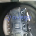
TI SN75LVDS83BDGGR
Bus Transmitters FlatLink 10-135MHz Transmitter


Brands: TI
Mfr.Part #: SN75LVDS83BDGGR
Datasheet: SN75LVDS83BDGGR Datasheet (PDF)
Package/Case: TSSOP56
Product Type: Interface - Specialized
RoHS Status:
Stock Condition: 50 pcs, New Original
Warranty: 1 Year Ovaga Warranty - Find Out More
0
1
Add To BomSN75LVDS83BDGGR General Description
The SN75LVDS83B FlatLink™ transmitter contains four 7-bit parallel-load serial-out shift registers, a 7X clock synthesizer, and five Low-Voltage Differential Signaling (LVDS) line drivers in a single integrated circuit. These functions allow 28 bits of single-ended LVTTL data to be synchronously transmitted over five balanced-pair conductors for receipt by a compatible receiver, such as the SN75LVDS82 and LCD panels with integrated LVDS receiver.
When transmitting, data bits D0 through D27 are each loaded into registers upon the edge of the input clock signal (CLKIN). The rising or falling edge of the clock can be selected via the clock select (CLKSEL) pin. The frequency of CLKIN is multiplied seven times, and then used to unload the data registers in 7-bit slices and serially. The four serial streams and a phase-locked clock (CLKOUT) are then output to LVDS output drivers. The frequency of CLKOUT is the same as the input clock, CLKIN.
The SN75LVDS83B requires no external components and little or no control. The data bus appears the same at the input to the transmitter and output of the receiver with the data transmission transparent to the user(s). The only user intervention is selecting a clock rising edge by inputting a high level to CLKSEL or a falling edge with a low-level input, and the possible use of the Shutdown/Clear (SHTDN). SHTDN is an active-low input to inhibit the clock, and shut off the LVDS output drivers for lower power consumption. A low-level on this signal clears all internal registers to a low-level.
The SN75LVDS83B is characterized for operation over ambient air temperatures of 10°C to 70°C.
Alternative device option: The SN75LVDS83A (SLLS980) is an alternative to the SN75LVDS83B for clock frequency range of 10MHz-100MHz only. The SN75LVDS83A is available in the TSSOP package option only.
Features
- LVDS Display Series Interfaces Directly to LCD
Display Panels With Integrated LVDS - Package Options: 4.5-mm × 7-mm BGA,
and 8.1-mm × 14-mm TSSOP - 1.8-V Up to 3.3-V Tolerant Data Inputs to Connect
Directly to Low-Power, Low-Voltage Application and
Graphic Processors - Transfer Rate up to 135 Mpps (Mega Pixel Per Second);
Pixel Clock Frequency Range 10 MHz to 135 MHz - Suited for Display Resolutions Ranging From HVGA
up to HD With Low EMI - Operates From a Single 3.3-V Supply and 170 mW (Typ.)
at 75 MHz - 28 Data Channels Plus Clock in Low-Voltage TTL to 4
Data Channels Plus Clock Out Low-Voltage Differential - Consumes Less Than 1 mW When Disabled
- Selectable Rising or Falling Clock Edge Triggered
Inputs - ESD: 5-kV HBM
- Support Spread Spectrum Clocking (SSC)
- Compatible with all OMAP™ 2x, OMAP™ 3x, and
DaVinci™ Application Processors
Specifications
| Parameter | Value | Parameter | Value |
|---|---|---|---|
| Protocols | Catalog | Rating | Catalog |
| Operating temperature range (°C) | -10 to 70 |
Shipping
| Shipping Type | Ship Fee | Lead Time | |
|---|---|---|---|
 |
DHL | $20.00-$40.00 (0.50 KG) | 2-5 days |
 |
Fedex | $20.00-$40.00 (0.50 KG) | 2-5 days |
 |
UPS | $20.00-$40.00 (0.50 KG) | 2-5 days |
 |
TNT | $20.00-$40.00 (0.50 KG) | 2-5 days |
 |
EMS | $20.00-$40.00 (0.50 KG) | 2-5 days |
 |
REGISTERED AIR MAIL | $20.00-$40.00 (0.50 KG) | 2-5 days |
Processing Time:Shipping fee depend on different zone and country.
Payment
| Terms of payment | Hand Fee | |
|---|---|---|
 |
Wire Transfer | charge US$30.00 banking fee. |
 |
Paypal | charge 4.0% service fee. |
 |
Credit Card | charge 3.5% service fee. |
 |
Western Union | charge US.00 banking fee. |
 |
Money Gram | charge US$0.00 banking fee. |
Guarantees
1.The electronic components you purchase include 365 Days Warranty, We guarantee product quality.
2.If some of the items you received aren't of perfect quality, we would resiponsibly arrange your refund or replacement. But the items must remain their orginal condition.
Packing
-

Step1 :Product
-

Step2 :Vacuum packaging
-

Step3 :Anti-static bag
-

Step4 :Individual packaging
-

Step5 :Packaging boxes
-

Step6 :bar-code shipping tag


All the products will packing in anti-staticbag. Ship with ESD antistatic protection.
Outside ESD packing’s lable will use ourcompany’s information: Part Mumber, Brand and Quantity.
We will inspect all the goods before shipment,ensure all the products at good condition and ensure the parts are new originalmatch datasheet.
After all the goods are ensure no problems afterpacking, we will packing safely and send by global express. It exhibitsexcellent puncture and tear resistance along with good seal integrity.


Part points
-
The SN75LVDS83BDGGR is a high-speed LVDS (low-voltage differential signaling) driver and receiver chip. It is designed to convert parallel video data into serial data, enabling the transmission of high-speed signals over long distances with low power consumption. The chip features a wide operating voltage range and can be used in various applications, including displays, video surveillance systems, and automotive electronics.
-
Equivalent
There are no direct equivalent products of the SN75LVDS83BDGGR chip from Texas Instruments. However, some alternatives in the same category of Low Voltage Differential Signaling (LVDS) transmitters are the DS90LV047A from Maxim Integrated and the ADV151 from Analog Devices. -
Features
The SN75LVDS83BDGGR is a serializer/deserializer (SerDes) IC that supports up to 24-bit video data transmission. It features low-voltage differential signaling (LVDS) technology for high-speed and low-power data transfer. The device operates over a wide temperature range and is suitable for automotive and industrial applications. -
Pinout
The SN75LVDS83BDGGR is a 40-pin LVDS driver that provides low-voltage differential signaling for flat panel displays. It includes six channels for data transmission and control signals, as well as power supply and ground pins. The device is commonly used in applications such as LCD displays, notebook computers, and LCD projectors. -
Manufacturer
Texas Instruments is the manufacturer of the SN75LVDS83BDGGR. It is a semiconductor manufacturing company that designs and manufactures electronic components, including integrated circuits used in various industries such as automotive, industrial, and consumer electronics. -
Application Field
The SN75LVDS83BDGGR has multiple application areas, including mobile phones, tablet computers, automotive electronics, industrial controllers, and medical equipment. -
Package
The SN75LVDS83BDGGR chip is available in a 48-pin TSSOP package type. It has a specific package form, which is relatively thin and flat with a small outline. The chip's package size is 9.7mm x 6.1mm.


We provide high quality products, thoughtful service and after sale guarantee
-

We have rich products, can meet your various needs.
-

Minimum order quantity starts from 1pcs.
-

Lowest international shipping fee starts from $0.00
-

365 days quality guarantee for all products