Images are for reference only See Product Specifications
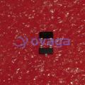
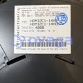
SM74611KTTR
Three 3-DDPAK/TO-263 packages


Brands: Texas Instruments
Mfr.Part #: SM74611KTTR
Datasheet: SM74611KTTR Datasheet (PDF)
Package/Case: TO-263 (KTT)-3
RoHS Status:
Stock Condition: 2875 pcs, New Original
Warranty: 1 Year Ovaga Warranty - Find Out More
0
1
Add To BomSM74611KTTR General Description
The SM74611 device is a smart bypass diode used in photovoltaic applications. The SM74611 device serves the purpose of providing an alternate path for string current when parts of the panel are shaded during normal operation. Without bypass diodes, the shaded cells will exhibit a hot spot which is caused by excessive power dissipation in the reverse biased cells.
Currently, conventional P-N junction diodes or Schottky diodes are used to mitigate this issue. Unfortunately the forward voltage drop for these diodes is still considered high (approximately 0.6 V for normal diodes and 0.4 V for Schottky). With 10 A of currents flowing through these diodes, the power dissipation can reach as high as 6 W. This in turn will raise the temperature inside the junction box where these diodes normally reside and reduce module reliability.
The advantage of the SM74611 is that it has a lower forward voltage drop than P-N junction and Schottky diodes. It has a typical average forward voltage drop of 26 mV at 8 A of current. This translates into typical power dissipation of 208 mW, which is significantly lower than the 3.2 W of conventional Schottky diodes. The SM74611 is also footprint and pin compatible with conventional D2PAK Schottky diodes, making it a drop-in replacement in many applications.
Features
- Maximum Reverse Voltage (VR) of 30 V
- Operating Forward Current (IF) of up to 15 A
- Low Average Forward Voltage (26 mV at 8 A)
- Less Power Dissipation than Schottky Diode
- Lower Leakage Current than Schottky Diode
- Footprint and Pin-Compatible With Conventional
D2PAK Schottky Diode - Operating Range (TJ) of –40°C to 125°C
Specifications
| Parameter | Value | Parameter | Value |
|---|---|---|---|
| Vin (min) (V) | 0.5 | Vin (max) (V) | 30 |
| Number of channels | 1 | Features | Reverse current blocking, Reverse polarity protection, Solar bypass |
| Iq (typ) (mA) | 0 | Iq (max) (mA) | 0 |
| FET | Integrated single blocking FET | Operating temperature range (°C) | -40 to 125 |
| IReverse (typ) (µA) | 3.3 | Design support | Simulation Model |
| Rating | Catalog | Imax (A) | 15 |
| Shutdown current (ISD) (mA) (A) | 0 | Device type | Smart bypass diode |
| Product type | Smart bypass diode |
Shipping
| Shipping Type | Ship Fee | Lead Time | |
|---|---|---|---|
 |
DHL | $20.00-$40.00 (0.50 KG) | 2-5 days |
 |
Fedex | $20.00-$40.00 (0.50 KG) | 2-5 days |
 |
UPS | $20.00-$40.00 (0.50 KG) | 2-5 days |
 |
TNT | $20.00-$40.00 (0.50 KG) | 2-5 days |
 |
EMS | $20.00-$40.00 (0.50 KG) | 2-5 days |
 |
REGISTERED AIR MAIL | $20.00-$40.00 (0.50 KG) | 2-5 days |
Processing Time:Shipping fee depend on different zone and country.
Payment
| Terms of payment | Hand Fee | |
|---|---|---|
 |
Wire Transfer | charge US$30.00 banking fee. |
 |
Paypal | charge 4.0% service fee. |
 |
Credit Card | charge 3.5% service fee. |
 |
Western Union | charge US.00 banking fee. |
 |
Money Gram | charge US$0.00 banking fee. |
Guarantees
1.The electronic components you purchase include 365 Days Warranty, We guarantee product quality.
2.If some of the items you received aren't of perfect quality, we would resiponsibly arrange your refund or replacement. But the items must remain their orginal condition.
Packing
-

Step1 :Product
-

Step2 :Vacuum packaging
-

Step3 :Anti-static bag
-

Step4 :Individual packaging
-

Step5 :Packaging boxes
-

Step6 :bar-code shipping tag


All the products will packing in anti-staticbag. Ship with ESD antistatic protection.
Outside ESD packing’s lable will use ourcompany’s information: Part Mumber, Brand and Quantity.
We will inspect all the goods before shipment,ensure all the products at good condition and ensure the parts are new originalmatch datasheet.
After all the goods are ensure no problems afterpacking, we will packing safely and send by global express. It exhibitsexcellent puncture and tear resistance along with good seal integrity.


We provide high quality products, thoughtful service and after sale guarantee
-

We have rich products, can meet your various needs.
-

Minimum order quantity starts from 1pcs.
-

Lowest international shipping fee starts from $0.00
-

365 days quality guarantee for all products