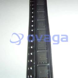
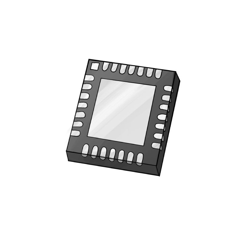
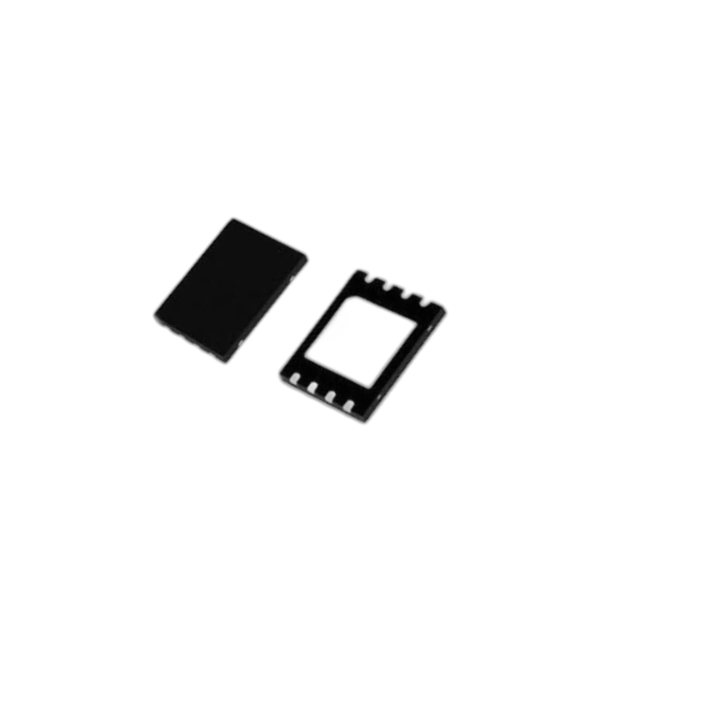
Images are for reference only See Product Specifications
vishay SI7489DP-T1-E3
SI7489DP-T1-E3 is a P-channel MOSFET transistor designed to handle up to 28 A of current and up to 100 V of voltage


Brands: Vishay
Mfr.Part #: SI7489DP-T1-E3
Datasheet: SI7489DP-T1-E3 Datasheet (PDF)
Package/Case: PowerPAK-SO-8
Product Type: MOSFET
RoHS Status:
Stock Condition: 6000 pcs, New Original
Warranty: 1 Year Ovaga Warranty - Find Out More
0
1
Add To BomSI7489DP-T1-E3 General Description
MOSFET P-CH 100V 28A PPAK SO-8
Features
Rds On (Max) @ Id, Vgs
41mOhm @ 7.8A, 10V
Power Dissipation (Max)
5.2W (Ta), 83W (Tc)
Drive Voltage (Max Rds On, Min Rds On)
4.5V, 10V
Input Capacitance (Ciss) (Max) @ Vds
4600 pF @ 50 V
Mfr
Vishay Siliconix
Vgs(th) (Max) @ Id
3V @ 250µA
Vgs (Max)
±20V
Drain to Source Voltage (Vdss)
100 V
Current - Continuous Drain (Id) @ 25°C
28A (Tc)
FET Type
P-Channel
Category
Discrete Semiconductor Products
Transistors
FETs, MOSFETs
Single FETs, MOSFETs
Gate Charge (Qg) (Max) @ Vgs
160 nC @ 10 V
Technology
MOSFET (Metal Oxide)
Operating Temperature
-55°C ~ 150°C (TJ)
Mounting Type
Surface Mount
Specifications
| Parameter | Value | Parameter | Value |
|---|---|---|---|
| feature-category | Power MOSFET | feature-material | |
| feature-process-technology | TrenchFET | feature-configuration | Single Quad Drain Triple Source |
| feature-channel-mode | Enhancement | feature-channel-type | P |
| feature-number-of-elements-per-chip | 1 | feature-maximum-drain-source-voltage-v | 100 |
| feature-maximum-gate-source-voltage-v | ±20 | feature-maximum-gate-threshold-voltage-v | |
| feature-maximum-continuous-drain-current-a | 28 | feature-maximum-drain-source-resistance-mohm | 41@10V |
| feature-typical-gate-charge-vgs-nc | 106@10V|[email protected] | feature-typical-gate-charge-10v-nc | 106 |
| feature-typical-input-capacitance-vds-pf | 4600@50V | feature-typical-output-capacitance-pf | |
| feature-maximum-power-dissipation-mw | 5200 | feature-packaging | Tape and Reel |
| feature-rad-hard | feature-pin-count | 8 | |
| feature-supplier-package | PowerPAK SO | feature-standard-package-name | |
| feature-cecc-qualified | No | feature-esd-protection | |
| feature-military | No | feature-aec-qualified | No |
| feature-aec-qualified-number | feature-eccn-code | EAR99 | |
| feature-svhc | No | feature-svhc-exceeds-threshold | No |
| Series | TrenchFET® | Product Status | Active |
| FET Type | P-Channel | Technology | MOSFET (Metal Oxide) |
| Drain to Source Voltage (Vdss) | 100 V | Current - Continuous Drain (Id) @ 25°C | 28A (Tc) |
| Drive Voltage (Max Rds On, Min Rds On) | 4.5V, 10V | Rds On (Max) @ Id, Vgs | 41mOhm @ 7.8A, 10V |
| Vgs(th) (Max) @ Id | 3V @ 250µA | Gate Charge (Qg) (Max) @ Vgs | 160 nC @ 10 V |
| Vgs (Max) | ±20V | Input Capacitance (Ciss) (Max) @ Vds | 4600 pF @ 50 V |
| Power Dissipation (Max) | 5.2W (Ta), 83W (Tc) | Operating Temperature | -55°C ~ 150°C (TJ) |
| Mounting Type | Surface Mount | Supplier Device Package | PowerPAK® SO-8 |
| Package / Case | PowerPAK® SO-8 |
Shipping
| Shipping Type | Ship Fee | Lead Time | |
|---|---|---|---|
 |
DHL | $20.00-$40.00 (0.50 KG) | 2-5 days |
 |
Fedex | $20.00-$40.00 (0.50 KG) | 2-5 days |
 |
UPS | $20.00-$40.00 (0.50 KG) | 2-5 days |
 |
TNT | $20.00-$40.00 (0.50 KG) | 2-5 days |
 |
EMS | $20.00-$40.00 (0.50 KG) | 2-5 days |
 |
REGISTERED AIR MAIL | $20.00-$40.00 (0.50 KG) | 2-5 days |
Processing Time:Shipping fee depend on different zone and country.
Payment
| Terms of payment | Hand Fee | |
|---|---|---|
 |
Wire Transfer | charge US$30.00 banking fee. |
 |
Paypal | charge 4.0% service fee. |
 |
Credit Card | charge 3.5% service fee. |
 |
Western Union | charge US.00 banking fee. |
 |
Money Gram | charge US$0.00 banking fee. |
Guarantees
1.The electronic components you purchase include 365 Days Warranty, We guarantee product quality.
2.If some of the items you received aren't of perfect quality, we would resiponsibly arrange your refund or replacement. But the items must remain their orginal condition.
Packing
-

Step1 :Product
-

Step2 :Vacuum packaging
-

Step3 :Anti-static bag
-

Step4 :Individual packaging
-

Step5 :Packaging boxes
-

Step6 :bar-code shipping tag


All the products will packing in anti-staticbag. Ship with ESD antistatic protection.
Outside ESD packing’s lable will use ourcompany’s information: Part Mumber, Brand and Quantity.
We will inspect all the goods before shipment,ensure all the products at good condition and ensure the parts are new originalmatch datasheet.
After all the goods are ensure no problems afterpacking, we will packing safely and send by global express. It exhibitsexcellent puncture and tear resistance along with good seal integrity.


Part points
-
The SI7489DP-T1-E3 chip is an electronic component developed by vishay siliconix. it is designed for power management applications and features a high-side load switch with overcurrent protection. the chip offers a low on-resistance and fast switching performance, making it suitable for various power control tasks in automotive, industrial, and consumer electronics.
-
Features
The SI7489DP-T1-E3 is a dual n-channel 30 v (d-s) mosfet designed for use in power management applications. it features low on-resistance, fast switching speed, and a small sot-363 package for space-constrained designs. additionally, it has a logic-level gate drive, making it compatible with low-voltage control signals. -
Pinout
The SI7489DP-T1-E3 is a dual n-channel mosfet. it has an 8-pin package, with the following pin configuration: 1 - source 1, 2 - drain 1, 3 - gate 1, 4 - nc, 5 - source 2, 6 - drain 2, 7 - gate 2, 8 - nc. -
Manufacturer
The manufacturer of the SI7489DP-T1-E3 is vishay siliconix. vishay siliconix is a company that specializes in the design, manufacture, and distribution of power and small-signal discrete semiconductors and passive electronic components. -
Application Field
The SI7489DP-T1-E3 is a voltage level translator ic. it can be used in various applications where voltage translation is required between different logic levels, such as communication interfaces, data converters, memory modules, and other digital systems.


We provide high quality products, thoughtful service and after sale guarantee
-

We have rich products, can meet your various needs.
-

Minimum order quantity starts from 1pcs.
-

Lowest international shipping fee starts from $0.00
-

365 days quality guarantee for all products


Recommend
-
![SQ2309ES]()
VISHAY
-
![SQJ457EP]()
-
![SQ2362ES]()
-
![SQ2361ES-T1-GE3]()
-
![SST112]()
-
![SUD40N06-25L]()