Images are for reference only See Product Specifications
TI OMAPL137DZKB3
Digital Signal Processors & Controllers - DSP, DSC C6000 DSP+ARM Processor


Brands: Texas Instruments
Mfr.Part #: OMAPL137DZKB3
Datasheet: OMAPL137DZKB3 Datasheet (PDF)
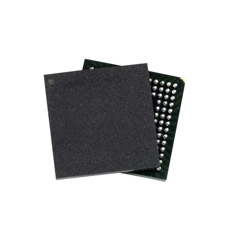
Package/Case: BGA-256
Product Type: Digital Signal Processors & Controllers - DSP, DSC
RoHS Status:
Stock Condition: 6554 pcs, New Original
Warranty: 1 Year Ovaga Warranty - Find Out More
0
1
Add To BomOMAPL137DZKB3 General Description
The OMAP-L137 device is a low-power applications processor based on an ARM926EJ-S and a TMS320C674x DSP core. It consumes significantly lower power than other members of the TMS320C6000 platform of DSPs.
The OMAP-L137 device enables original-equipment manufacturers (OEMs) and original-design manufacturers (ODMs) to quickly bring to market devices featuring robust operating systems support, rich user interfaces, and high processing performance life through the maximum flexibility of a fully integrated mixed processor solution.
The dual-core architecture of the OMAP-L137 device provides benefits of both DSP and Reduced Instruction Set Computer (RISC) technologies, incorporating a high-performance TMS320C674x DSP core and an ARM926EJ-S core.
The ARM926EJ-S is a 32-bit RISC processor core that performs 32-bit or 16-bit instructions and processes 32-bit, 16-bit, or 8-bit data. The core uses pipelining so that all parts of the processor and memory system can operate continuously.
The ARM core has a coprocessor 15 (CP15), protection module, and data and program Memory Management Units (MMUs) with table look-aside buffers. The ARM core has separate 16-KB instruction and 16KB of data caches. Both memory blocks are four-way associative with virtual index virtual tag (VIVT). The ARM core also has 8KB of RAM (Vector Table) and 64KB of ROM.
The OMAP-L137 DSP core uses a two-level cache-based architecture. The Level 1 program cache (L1P) is a 32-KB direct mapped cache and the Level 1 data cache (L1D) is a 32-KB 2-way set-associative cache. The Level 2 program cache (L2P) consists of a 256-KB memory space that is shared between program and data space. L2 memory can be configured as mapped memory, cache, or combinations of the two. Although the DSP L2 is accessible by ARM and other hosts in the system, an additional 128KB of RAM shared memory is available for use by other hosts without affecting DSP performance.
The peripheral set includes: a 10/100 Mbps Ethernet MAC (EMAC) with a management data input/output (MDIO) module; two I2C Bus interfaces; 3 multichannel audio serial ports (McASPs) with 16/12/4 serializers and FIFO buffers; two 64-bit general-purpose timers each configurable (one configurable as watchdog); a configurable 16-bit host-port interface (HPI); up to 8 banks of 16 pins of general-purpose input/output (GPIO) with programmable interrupt/event generation modes, multiplexed with other peripherals; 3 UART interfaces (one with both RTS and CTS); three enhanced high-resolution pulse width modulator (eHRPWM) peripherals; three 32-bit enhanced capture (eCAP) module peripherals which can be configured as 3 capture inputs or 3 auxiliary pulse width modulator (APWM) outputs; two 32-bit enhanced quadrature encoded pulse (eQEP) peripherals; and 2 external memory interfaces: an asynchronous and SDRAM external memory interface (EMIFA) for slower memories or peripherals, and a higher speed memory interface (EMIFB) for SDRAM.
The Ethernet Media Access Controller (EMAC) provides an efficient interface between the OMAP-L137 device and the network. The EMAC supports both 10Base-T and 100Base-TX, or 10 Mbps and 100 Mbps in either half- or full-duplex mode. Additionally, an MDIO interface is available for PHY configuration.
The HPI, I2C, SPI, USB1.1, and USB2.0 ports allow the OMAP-L137 device to easily control peripheral devices and/or communicate with host processors.
The rich peripheral set provides the ability to control external peripheral devices and communicate with external processors. For details on each of the peripherals, see the related sections later in this document and the associated peripheral reference guides.
The OMAP-L137 device has a complete set of development tools for both the ARM and DSP. These include C compilers, a DSP assembly optimizer to simplify programming and scheduling, and a Windows® debugger interface for visibility into source code execution.
Features
- Software Support
- TI DSP/BIOS
- Chip Support Library and DSP Library
- Dual Core SoC
- 375- and 456-MHz ARM926EJ-S RISC MPU
- 375- and 456-MHz C674x VLIW DSP
- ARM926EJ-S Core
- 32-Bit and 16-Bit (Thumb®) Instructions
- DSP Instruction Extensions
- Single Cycle MAC
- ARM® Jazelle® Technology
- Embedded ICE-RT™ for Real-Time Debug
- ARM9™ Memory Architecture
- 16KB of Instruction Cache
- 16KB of Data Cache
- 8KB of RAM (Vector Table)
- 64KB of ROM
- C674x Instruction Set Features
- Superset of the C67x+ and C64x+ ISAs
- Up to 3648 MIPS and 2736 MFLOPS C674x
- Byte-Addressable (8-, 16-, 32-, and 64-Bit Data)
- 8-Bit Overflow Protection
- Bit-Field Extract, Set, Clear
- Normalization, Saturation, Bit-Counting
- Compact 16-Bit Instructions
- C674x Two-Level Cache Memory Architecture
- 32KB of L1P Program RAM/Cache
- 32KB of L1D Data RAM/Cache
- 256KB of L2 Unified Mapped RAM/Cache
- Flexible RAM/Cache Partition (L1 and L2)
- Enhanced Direct Memory Access Controller 3 (EDMA3):
- 2 Transfer Controllers
- 32 Independent DMA Channels
- 8 Quick DMA Channels
- Programmable Transfer Burst Size
- TMS320C674x Fixed- and Floating-Point VLIW DSP Core
- Load-Store Architecture with Nonaligned Support
- 64 General-Purpose Registers (32-Bit)
- Six ALU (32- and 40-Bit) Functional Units
- Supports 32-Bit Integer, SP (IEEE Single Precision/32-Bit) and DP (IEEE Double Precision/64-Bit) Floating Point
- Supports up to Four SP Additions Per Clock, Four DP Additions Every 2 Clocks
- Supports up to Two Floating-Point (SP or DP) Reciprocal Approximation (RCPxP) and Square-Root Reciprocal Approximation (RSQRxP) Operations Per Cycle
- Two Multiply Functional Units
- Mixed-Precision IEEE Floating Point Multiply Supported up to:
- 2 SP x SP -> SP Per Clock
- 2 SP x SP -> DP Every Two Clocks
- 2 SP x DP -> DP Every Three Clocks
- 2 DP x DP -> DP Every Four Clocks
- Fixed-Point Multiply Supports Two 32 x 32-Bit Multiplies, Four 16 x 16-Bit Multiplies, or Eight 8 x 8-Bit Multiplies per Clock Cycle, and Complex Multiples
- Mixed-Precision IEEE Floating Point Multiply Supported up to:
- Instruction Packing Reduces Code Size
- All Instructions Conditional
- Hardware Support for Modulo Loop
Operation - Protected Mode Operation
- Exceptions Support for Error Detection and Program Redirection
- 128KB of RAM Shared Memory
- 3.3-V LVCMOS I/Os (Except for USB Interfaces)
- Two External Memory Interfaces:
- EMIFA
- NOR (8- or 16-Bit-Wide Data)
- NAND (8- or 16-Bit-Wide Data)
- 16-Bit SDRAM with 128-MB Address Space
- EMIFB
- 32-Bit or 16-Bit SDRAM with 256-MB Address Space
- EMIFA
- Three Configurable 16550-Type UART Modules:
- UART0 with Modem Control Signals
- Autoflow Control Signals (CTS, RTS) on UART0 Only
- 16-Byte FIFO
- 16x or 13x Oversampling Option
- LCD Controller
- Two Serial Peripheral Interfaces (SPIs) Each with One Chip Select
- Multimedia Card (MMC)/Secure Digital (SD) Card Interface with Secure Data I/O (SDIO)
- Two Master and Slave Inter-Integrated Circuit (I2C Bus™)
- One Host-Port Interface (HPI) with 16-Bit-Wide Muxed Address/Data Bus for High Bandwidth
- Programmable Real-Time Unit Subsystem (PRUSS)
- Two Independent Programmable Realtime Unit (PRU) Cores
- 32-Bit Load and Store RISC Architecture
- 4KB of Instruction RAM per Core
- 512 Bytes of Data RAM per Core
- PRUSS can be Disabled via Software to Save Power
- Standard Power-Management Mechanism
- Clock Gating
- Entire Subsystem Under a Single PSC Clock Gating Domain
- Dedicated Interrupt Controller
- Dedicated Switched Central Resource
- Two Independent Programmable Realtime Unit (PRU) Cores
- USB 1.1 OHCI (Host) with Integrated PHY (USB1)
- USB 2.0 OTG Port with Integrated PHY (USB0)
- USB 2.0 High- and Full-Speed Client
- USB 2.0 High-, Full-, and Low-Speed Host
- End Point 0 (Control)
- End Points 1,2,3,4 (Control, Bulk, Interrupt or ISOC) RX and TX
- Three Multichannel Audio Serial Ports (McASPs):
- Six Clock Zones and 28 Serial Data Pins
- Supports TDM, I2S, and Similar Formats
- DIT-Capable (McASP2)
- FIFO Buffers for Transmit and Receive
- 10/100 Mbps Ethernet MAC (EMAC):
- IEEE 802.3 Compliant (3.3-V I/O Only)
- RMII Media-Independent Interface
- Management Data I/O (MDIO) Module
- Real-Time Clock with 32-kHz Oscillator and Separate Power Rail
- One 64-Bit General-Purpose Timer (Configurable as Two 32-Bit Timers)
- One 64-Bit General-Purpose Watchdog Timer (Configurable as Two 32-Bit General-Purpose Timers)
- Three Enhanced Pulse Width Modulators (eHRPWMs):
- Dedicated 16-Bit Time-Base Counter with Period and Frequency Control
- 6 Single Edge, 6 Dual Edge Symmetric, or 3 Dual Edge Asymmetric Outputs
- Dead-Band Generation
- PWM Chopping by High-Frequency Carrier
- Trip Zone Input
- Three 32-Bit Enhanced Capture (eCAP) Modules:
- Configurable as 3 Capture Inputs or 3 Auxiliary Pulse Width Modulator (APWM) Outputs
- Single-Shot Capture of up to Four Event Time-Stamps
- Two 32-Bit Enhanced Quadrature Encoder Pulse (eQEP) Modules
- 256-Ball Pb-Free Plastic Ball Grid Array (PBGA) [ZKB Suffix], 1.0-mm Ball Pitch
- Commercial, Industrial, Extended, or Automotive Temperature
Specifications
| Parameter | Value | Parameter | Value |
|---|---|---|---|
| Manufacturer | Texas Instruments | Product Category | Digital Signal Processors & Controllers - DSP, DSC |
| RoHS | Details | Product | DSPs |
| Series | OMAP-L137 | Tradename | OMAP Application Processor |
| Mounting Style | SMD/SMT | Package / Case | BGA-256 |
| Core | ARM926EJ-S, C674x | Number of Cores | 2 Core |
| Maximum Clock Frequency | 375 MHz, 375 MHz | L1 Cache Instruction Memory | 16 kB, 32 kB |
| L1 Cache Data Memory | 16 kB, 32 kB | Program Memory Size | 32 kB |
| Data RAM Size | 8 kB | Operating Supply Voltage | 1.14 V to 1.32 V |
| Minimum Operating Temperature | - 40 C | Maximum Operating Temperature | + 125 C |
| Packaging | ["Tray"] | Brand | Texas Instruments |
| Data Bus Width | 16 bit | Development Kit | TMDSOSKL137 |
| Instruction Type | Fixed/Floating Point | Interface Type | SPI, USB |
| Moisture Sensitive | Yes | Number of Timers/Counters | 1 Timer |
| Product Type | DSP - Digital Signal Processors & Controllers | Program Memory Type | Cache |
| Factory Pack Quantity | 90 | Subcategory | Embedded Processors & Controllers |
| Supply Voltage - Min | 1.14 V | Unit Weight | 0.098203 oz |
| Arm CPU | 1 Arm9 | Arm (max) (MHz) | 456 |
| Coprocessors | C674x DSP | CPU | 32-bit |
| Display type | 1 LCD | Protocols | Ethernet |
| Ethernet MAC | 1-Port 10/100 | Hardware accelerators | PRUSS |
| Operating system | Linux, RTOS | Security | Device identity, Memory protection |
| Rating | Catalog | Power supply solution | TPS65910 |
| Operating temperature range (°C) | -40 to 105, -40 to 125, -40 to 90, 0 to 90 |
Shipping
| Shipping Type | Ship Fee | Lead Time | |
|---|---|---|---|
 |
DHL | $20.00-$40.00 (0.50 KG) | 2-5 days |
 |
Fedex | $20.00-$40.00 (0.50 KG) | 2-5 days |
 |
UPS | $20.00-$40.00 (0.50 KG) | 2-5 days |
 |
TNT | $20.00-$40.00 (0.50 KG) | 2-5 days |
 |
EMS | $20.00-$40.00 (0.50 KG) | 2-5 days |
 |
REGISTERED AIR MAIL | $20.00-$40.00 (0.50 KG) | 2-5 days |
Processing Time:Shipping fee depend on different zone and country.
Payment
| Terms of payment | Hand Fee | |
|---|---|---|
 |
Wire Transfer | charge US$30.00 banking fee. |
 |
Paypal | charge 4.0% service fee. |
 |
Credit Card | charge 3.5% service fee. |
 |
Western Union | charge US.00 banking fee. |
 |
Money Gram | charge US$0.00 banking fee. |
Guarantees
1.The electronic components you purchase include 365 Days Warranty, We guarantee product quality.
2.If some of the items you received aren't of perfect quality, we would resiponsibly arrange your refund or replacement. But the items must remain their orginal condition.
Packing
-

Step1 :Product
-

Step2 :Vacuum packaging
-

Step3 :Anti-static bag
-

Step4 :Individual packaging
-

Step5 :Packaging boxes
-

Step6 :bar-code shipping tag


All the products will packing in anti-staticbag. Ship with ESD antistatic protection.
Outside ESD packing’s lable will use ourcompany’s information: Part Mumber, Brand and Quantity.
We will inspect all the goods before shipment,ensure all the products at good condition and ensure the parts are new originalmatch datasheet.
After all the goods are ensure no problems afterpacking, we will packing safely and send by global express. It exhibitsexcellent puncture and tear resistance along with good seal integrity.


We provide high quality products, thoughtful service and after sale guarantee
-

We have rich products, can meet your various needs.
-

Minimum order quantity starts from 1pcs.
-

Lowest international shipping fee starts from $0.00
-

365 days quality guarantee for all products