


Images are for reference only See Product Specifications
Microchip MEC1527H-B0-I/TF
Embedded Controller with Flash.Embedded Controller.


Brands: Microchip Technology, Inc
Mfr.Part #: MEC1527H-B0-I/TF
Datasheet: MEC1527H-B0-I/TF Datasheet (PDF)
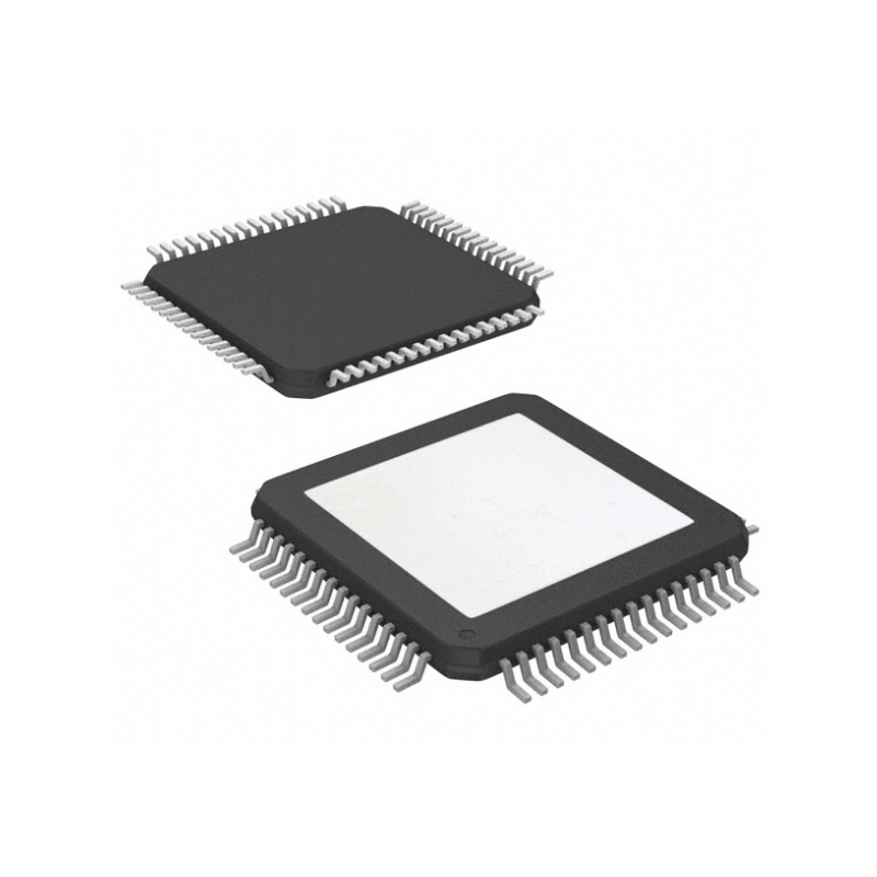
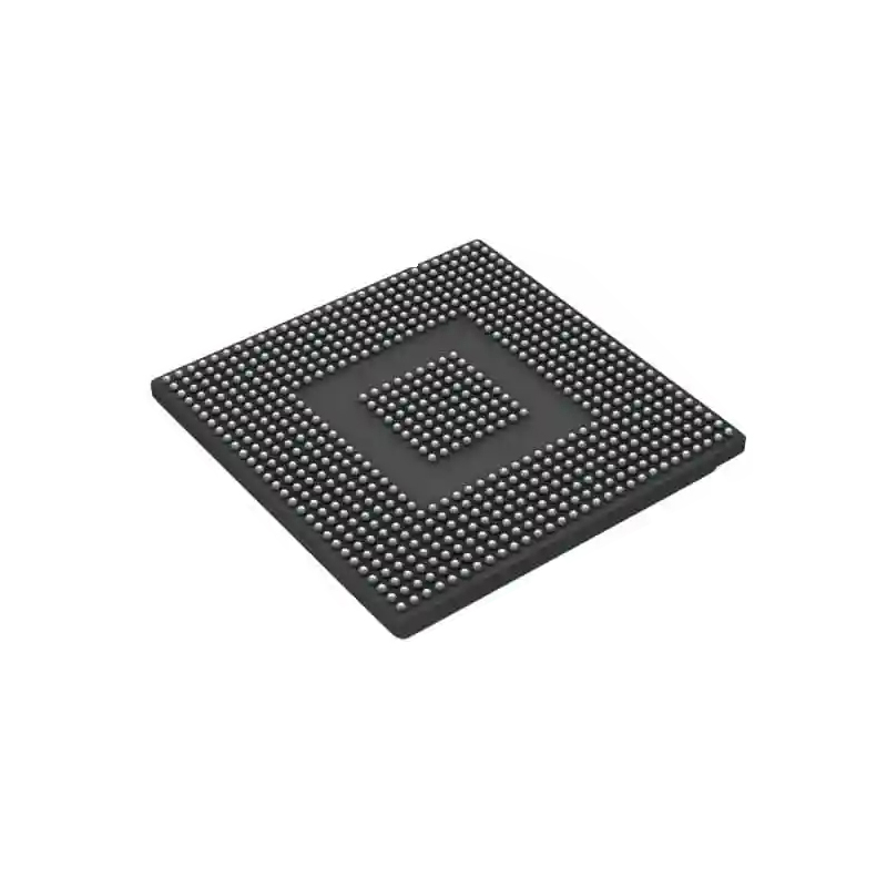
Package/Case: WFBGA
Product Type: ARM Microcontrollers - MCU
RoHS Status:
Stock Condition: 3482 pcs, New Original
Warranty: 1 Year Ovaga Warranty - Find Out More
0
1
Add To BomMEC1527H-B0-I/TF General Description
The MEC152x is a family of low power integrated embedded controllers designed for notebook applications. The MEC152x is a highly-configurable, mixed-signal, advanced I/O controller architecture. It contains a 32-bit ARM® CortexM4 processor core with closely-coupled memory for optimal code execution and data access. Unique to the MEC1527 is a 4Mbit in-chip SPI Serial Flash. An internal ROM, embedded in the design, is used to store the power on/boot sequence and APIs available during run time. When VTR_CORE is applied to the device, the secure boot loader API is used to download the custom firmware image from the system’s shared SPI Flash device, thereby allowing system designers to customize the device’s behavior.
The MEC152x device is directly powered by a minimum of two separate suspend supply planes (VBAT and VTR) and senses a third runtime power plane (VCC) to provide “instant on” and system power management functions. The MEC152x has two banks of I/O pins that are able to operate at either 3.3 V or 1.8 V. Operating at 1.8V allows the MEC152x to interface with the latest platform controller hubs and will lower the overall power consumed by the device, whereas 3.3V allows this device to be integrated into legacy platforms that require 3.3V operation.
The MEC152x host interface is the Intel® Enhanced Serial Peripheral Interface (eSPI). The eSPI Interface is a 1.8V interface that operates in single, double and quad I/O modes. The eSPI Interface supports all four eSPI channels: Peripheral Channel, Virtual Wires Channel, OOB Message Channel, and Run-time Flash Access Channel. The eSPI hardware Flash Access Channel is used by the Boot ROM to support Master Attached Flash Sharing (MAFS). In addition, the MEC152x has specially designed hardware to support Slave Attached Flash Sharing (SAFS). The eSPI SAFS Bridge imposes Region-Based Protection and Locking security feature, which limits access to certain regions of the flash to specific masters. There may be one or more masters (e.g., BIOS, ME, etc) that will access the SAF via the eSPI interface. The ARM® Cortex-M4 processor is also considered a master, which will also have its access limited to EC only regions of SPI Flash as determined by the customer firmware application.
The MEC152x secure boot loader authenticates and optionally decrypts the SPI Flash OEM boot image using the AES256, ECDSA , SHA-384 cryptographic hardware accelerators. The MEC152x hardware accelerators support 128-bit and 256-bit AES encryption, ECDSA and EC_KCDSA signing algorithms, 1024-bits to 4096-bits RSA and Elliptic asymmetric public key algorithms, and a True Random Number Generator (TRNG). Runtime APIs are provided in the ROM for customer application code to use the cryptographic hardware. Additionally, the device offers lockable OTP storage for private keys and IDs.
The MEC152x is designed to be incorporated into low power PC architecture designs and supports ACPI sleep states (S0-S5). During normal operation, the hardware always operates in the lowest power state for a given configuration. The chip power management logic offers two low power states: light sleep and heavy sleep. These features can be used to support S0 Connected Standby state and the lower ACPI S3-S5 system sleep states. In connected standby, any eSPI command will wake the device and be processed. When the chip is sleeping, it has many wake events that can be configured to return the device to normal operation. Some examples of supported wake events are PS2 wake events, RTC, Week Alarm, Hibernation Timer, or any GPIO pin.
The MEC152x offers a software development system interface that includes a Trace FIFO Debug port, a host accessible serial debug port with a 16C550A register interface, a Port 80 BIOS Debug Port, and a 2-pin Serial Wire Debug (SWD) interface. Also included is a 4-wire JTAG interface used for Boundary Scan testing.

Specifications
| Parameter | Value | Parameter | Value |
|---|---|---|---|
| Keyboard Scan Matrix | 18x8 | UART | 3 |
| Customer Programmable RAM | Yes | Host Interface | eSPI, LPC, I2C |
| Crypto Engine | Yes | Code Storage | 256 KB (Code + Data) |
| Operating Temperature | -40C to +85C | PCH Temp Monitoring | Yes |
| Low Power Timers | 0 | Tach | 4 |
| Deep Sleep S5 | Yes | Fan Tachometer Inputs | 4 |
| Max Operating Frequency | 48 MHz | 8024 Keyboard Controller | Yes |
| PCI Resets | 1 | PECI Support | Yes |
| Data RAM | 32 KB | HW Auto Fan Controller | 0 |
| Breathing/ Blinking LED | 3 | Legacy I/O | Yes |
| GPIO | 108 | PWM | 9 |
| Package | 144-WFBGA (SZ) | VBAT-Powered, Power Control Interface | 3 |
| LED | 3 | SMBus Interface | Yes |
| Analog to Digital Converter | 8 | Capture/_Compare | 6 |
| Temp Monitoring | 1 | SMBus Ports | 15 |
| BC Link | 0 | SPI_Host | 1 |
| Flash/Code RAM | 256 | EEPROM | 0 |
| AMD SB-TSI | 1 | PECI | 1 |
| ACPI Interfaces | 5 | Counter/Timers | 3 |
| feature-category | feature-process-technology | ||
| feature-minimum-operating-supply-voltage-v | feature-maximum-supply-current-a | ||
| feature-maximum-operating-supply-voltage-v | feature-packaging | ||
| feature-pin-count | 128 | feature-supplier-package | WFBGA |
| feature-standard-package-name1 | feature-cecc-qualified | ||
| feature-esd-protection | feature-military | ||
| feature-aec-qualified | feature-aec-qualified-number | ||
| feature-auto-motive | feature-p-pap | ||
| feature-eccn-code | EAR99 | feature-svhc | |
| feature-svhc-exceeds-threshold | No |
Shipping
| Shipping Type | Ship Fee | Lead Time | |
|---|---|---|---|
 |
DHL | $20.00-$40.00 (0.50 KG) | 2-5 days |
 |
Fedex | $20.00-$40.00 (0.50 KG) | 2-5 days |
 |
UPS | $20.00-$40.00 (0.50 KG) | 2-5 days |
 |
TNT | $20.00-$40.00 (0.50 KG) | 2-5 days |
 |
EMS | $20.00-$40.00 (0.50 KG) | 2-5 days |
 |
REGISTERED AIR MAIL | $20.00-$40.00 (0.50 KG) | 2-5 days |
Processing Time:Shipping fee depend on different zone and country.
Payment
| Terms of payment | Hand Fee | |
|---|---|---|
 |
Wire Transfer | charge US$30.00 banking fee. |
 |
Paypal | charge 4.0% service fee. |
 |
Credit Card | charge 3.5% service fee. |
 |
Western Union | charge US.00 banking fee. |
 |
Money Gram | charge US$0.00 banking fee. |
Guarantees
1.The electronic components you purchase include 365 Days Warranty, We guarantee product quality.
2.If some of the items you received aren't of perfect quality, we would resiponsibly arrange your refund or replacement. But the items must remain their orginal condition.
Packing
-

Step1 :Product
-

Step2 :Vacuum packaging
-

Step3 :Anti-static bag
-

Step4 :Individual packaging
-

Step5 :Packaging boxes
-

Step6 :bar-code shipping tag


All the products will packing in anti-staticbag. Ship with ESD antistatic protection.
Outside ESD packing’s lable will use ourcompany’s information: Part Mumber, Brand and Quantity.
We will inspect all the goods before shipment,ensure all the products at good condition and ensure the parts are new originalmatch datasheet.
After all the goods are ensure no problems afterpacking, we will packing safely and send by global express. It exhibitsexcellent puncture and tear resistance along with good seal integrity.


We provide high quality products, thoughtful service and after sale guarantee
-

We have rich products, can meet your various needs.
-

Minimum order quantity starts from 1pcs.
-

Lowest international shipping fee starts from $0.00
-

365 days quality guarantee for all products


Recommend
-
![PIC24FV32KA302-I/SO]()
-
![PIC24FJ64GA306-I/PT]()
-
![PIC24EP256GP204-I/PT]()
Microchip Technology, Inc
16-bit Microcontrollers - MCU 16B 256KB FL 32KBR 6...
-
![PIC24F32KA304-I/PT]()
-
![PIC24F32KA304-I/ML]()
-
![PIC24FJ128GA306-I/PT]()


