Images are for reference only See Product Specifications
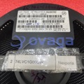
NEXPERIA LSF0108PW-Q100J
Voltage Level Translator Bidirectional 1 Circuit 8 Channel 100MHz 20-TSSOP


Brands: Nexperia
Mfr.Part #: LSF0108PW-Q100J
Datasheet: LSF0108PW-Q100J Datasheet (PDF)
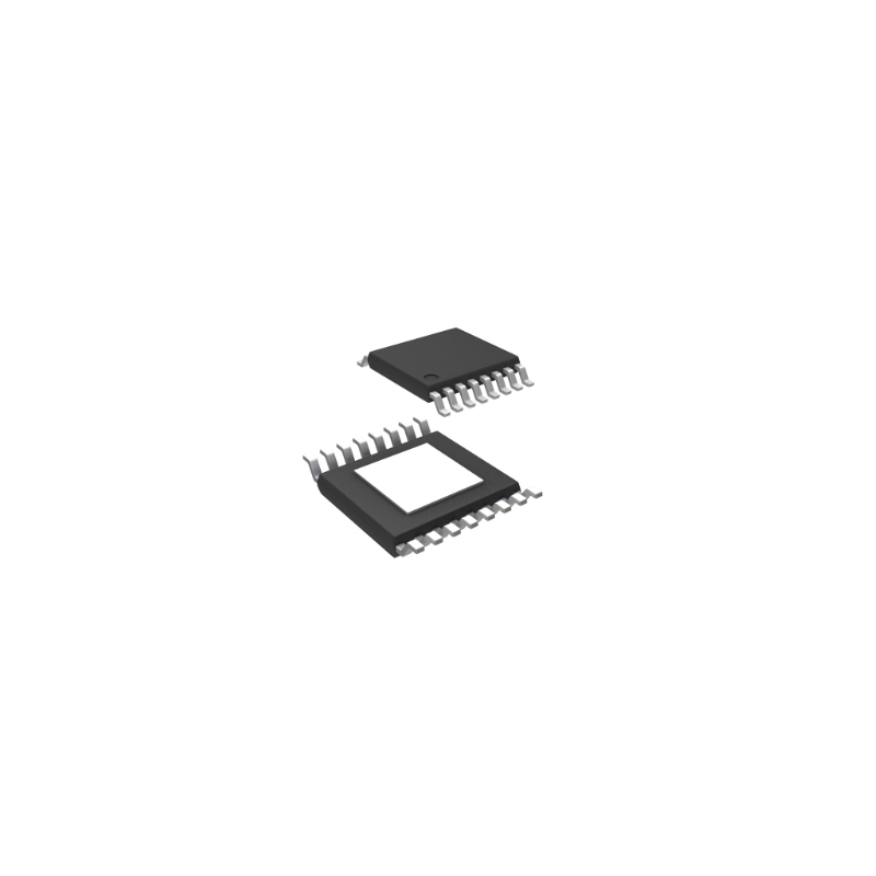
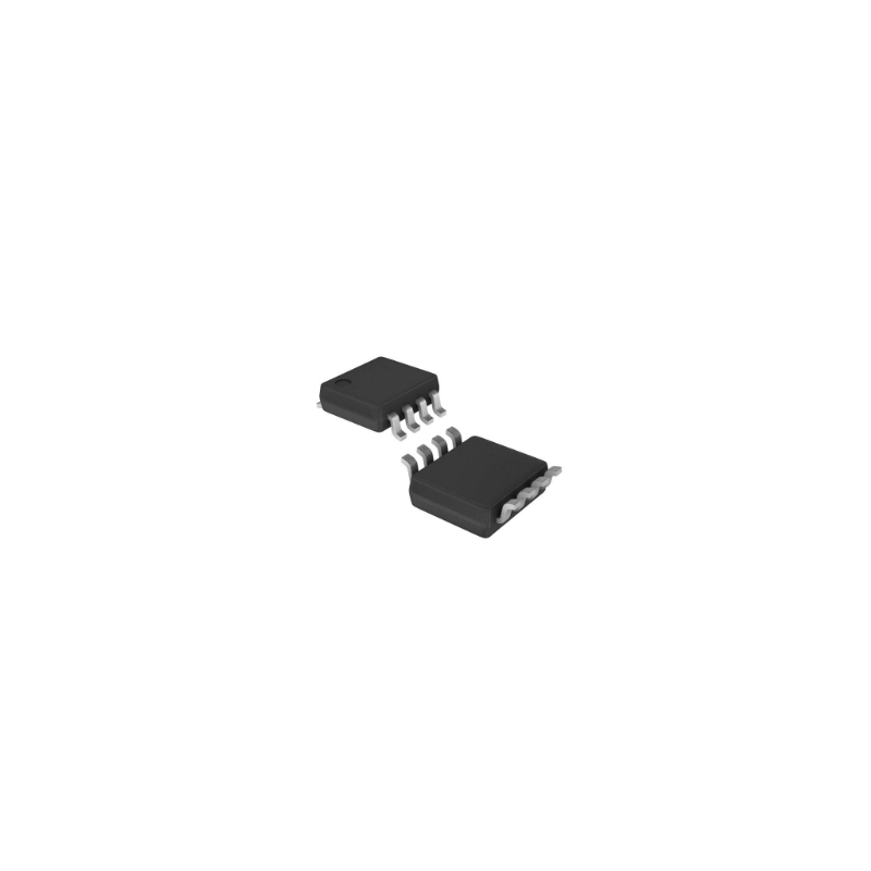
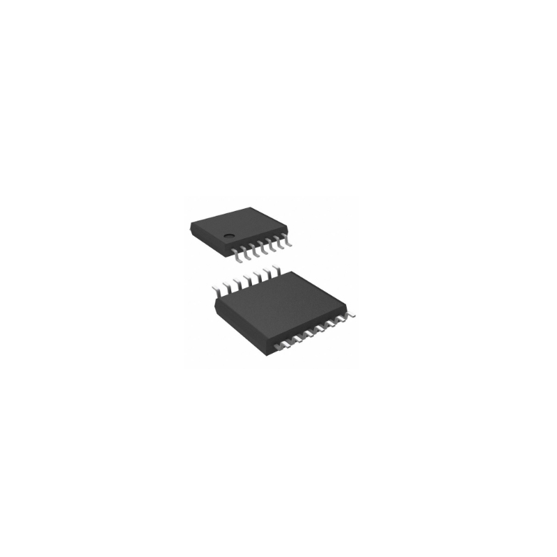
Package/Case: TSSOP-20
Product Type: Translation - Voltage Levels
RoHS Status:
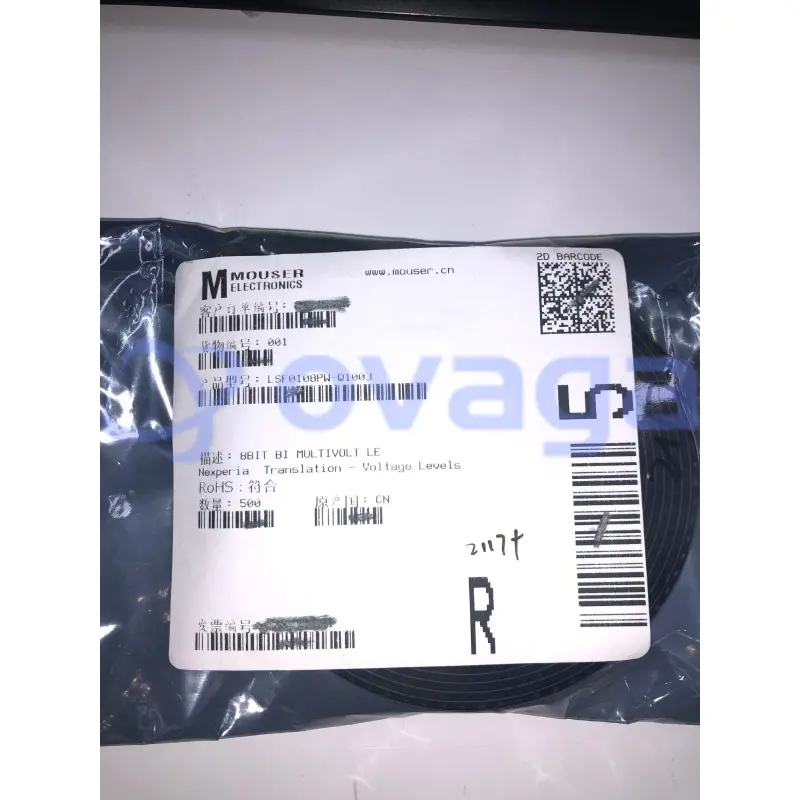
Stock Condition: 9458 pcs, New Original
Warranty: 1 Year Ovaga Warranty - Find Out More
0
1
Add To BomLSF0108PW-Q100J General Description
The LSF0108-Q100 is an 8 Channel bidirectional multi-voltage level translator for open-drain and push-pull applications. It supports up to 100 MHz up translation and ≥ 100 MHz down translation at ≤ 30 pF capacitive load. There is no need for a direction pin which minimizes system effort. The LSF0108-Q100 supports 5 V tolerant I/O pins for compatibility with TTL levels in a variety of applications. The ability to set up different voltage translation levels on each channel makes the device very flexible and suitable for a lot of different applications.This product has been qualified to the Automotive Electronics Council (AEC) standard Q100 (Grade 1) and is suitable for use in automotive applications.
Features
- Automotive product qualification in accordance with AEC-Q100 (Grade 1)Specified from -40 °C to +125 °C
- Specified from -40 °C to +125 °C
- Bidirectional voltage translation with no direction pin
- Up translation≤ 100 MHz; CL = 30 pF≤ 40 MHz; CL = 50 pF
- ≤ 100 MHz; CL = 30 pF
- ≤ 40 MHz; CL = 50 pF
- Down translation≥ 100 MHz; CL = 30 pF≤ 40 MHz; CL = 50 pF
- ≥ 100 MHz; CL = 30 pF
- ≤ 40 MHz; CL = 50 pF
- Hot insertion
- Bidirectional voltage level translation between:0.95 V and 1.8 V, 2.5 V, 3.3 V and 5.0 V1.2 V and 1.8 V, 2.5 V, 3.3 V and 5.0 V1.8 V and 2.5 V, 3.3 V and 5.0 V2.5 V and 3.3 V and 5.0 V3.3 V and 5.0 V
- 0.95 V and 1.8 V, 2.5 V, 3.3 V and 5.0 V
- 1.2 V and 1.8 V, 2.5 V, 3.3 V and 5.0 V
- 1.8 V and 2.5 V, 3.3 V and 5.0 V
- 2.5 V and 3.3 V and 5.0 V
- 3.3 V and 5.0 V
- Low standby current
- 5 V tolerant I/O pins to support TTL
- Low RON provides less signal distortion
- High-impedance I/O pins for EN = Low.
- Flow-through pinout for easy PCB trace routing.
- Latch-up performance exceeds 100 mA per JESD78 class II level A
- ESD protection:HBM ANSI/ESDA/JEDEC JS-001 exceeds 2000 VCDM ANSI/ESDA/JEDEC JS-002 exceeds 1000 V
- HBM ANSI/ESDA/JEDEC JS-001 exceeds 2000 V
- CDM ANSI/ESDA/JEDEC JS-002 exceeds 1000 V
- DHVQFN package with Side-Wettable Flanks enabling Automatic Optical Inspection (AOI) of solder joints
Application
- GPIO, MDIO, PMBus, SMBus, SDIO, UART, I²C, and other interfaces in Telecom infrastructure
- Industrial
- Personal computing
- Automotive

Specifications
| Parameter | Value | Parameter | Value |
|---|---|---|---|
| Manufacturer: | Nexperia | Product Category: | Translation - Voltage Levels |
| RoHS: | Details | Type: | Bidirectional Multi-Voltage Level Translator |
| Mounting Style: | SMD/SMT | Package / Case: | TSSOP-20 |
| Supply Voltage - Min: | 0 V | Supply Voltage - Max: | 5 V |
| Minimum Operating Temperature: | - 40 C | Maximum Operating Temperature: | + 125 C |
| Propagation Delay Time: | 1.9 ns, 2 ns | Qualification: | AEC-Q100 |
| Packaging: | MouseReel | Brand: | Nexperia |
| Number of Channels: | 8 Channel | Operating Supply Current: | 64 mA |
| Pd - Power Dissipation: | 500 mW | Product Type: | Translation - Voltage Levels |
| Factory Pack Quantity: | 2500 | Subcategory: | Logic ICs |
| Part # Aliases: | 935690918118 |
Shipping
| Shipping Type | Ship Fee | Lead Time | |
|---|---|---|---|
 |
DHL | $20.00-$40.00 (0.50 KG) | 2-5 days |
 |
Fedex | $20.00-$40.00 (0.50 KG) | 2-5 days |
 |
UPS | $20.00-$40.00 (0.50 KG) | 2-5 days |
 |
TNT | $20.00-$40.00 (0.50 KG) | 2-5 days |
 |
EMS | $20.00-$40.00 (0.50 KG) | 2-5 days |
 |
REGISTERED AIR MAIL | $20.00-$40.00 (0.50 KG) | 2-5 days |
Processing Time:Shipping fee depend on different zone and country.
Payment
| Terms of payment | Hand Fee | |
|---|---|---|
 |
Wire Transfer | charge US$30.00 banking fee. |
 |
Paypal | charge 4.0% service fee. |
 |
Credit Card | charge 3.5% service fee. |
 |
Western Union | charge US.00 banking fee. |
 |
Money Gram | charge US$0.00 banking fee. |
Guarantees
1.The electronic components you purchase include 365 Days Warranty, We guarantee product quality.
2.If some of the items you received aren't of perfect quality, we would resiponsibly arrange your refund or replacement. But the items must remain their orginal condition.
Packing
-

Step1 :Product
-

Step2 :Vacuum packaging
-

Step3 :Anti-static bag
-

Step4 :Individual packaging
-

Step5 :Packaging boxes
-

Step6 :bar-code shipping tag


All the products will packing in anti-staticbag. Ship with ESD antistatic protection.
Outside ESD packing’s lable will use ourcompany’s information: Part Mumber, Brand and Quantity.
We will inspect all the goods before shipment,ensure all the products at good condition and ensure the parts are new originalmatch datasheet.
After all the goods are ensure no problems afterpacking, we will packing safely and send by global express. It exhibitsexcellent puncture and tear resistance along with good seal integrity.


Part points
-
The LSF0108PW-Q100J is a low-power, high-speed octal bus switch with an operating voltage range of 1.65V to 3.6V. It features 5Ω switch impedance, minimal propagation delay, and low quiescent power dissipation. This chip is designed for high-performance applications requiring minimal power consumption and fast switching speeds.
-
Equivalent
The equivalent products of the LSF0108PW-Q100J chip include the LSF0108PW-Q1J, LSF0108PW-Q1, LSF0108PW-Q100, LSF0108PW, and LSF0121PW-Q100J chips. These chips are all in the same family of voltage level translators with similar specifications and features. -
Features
LSF0108PW-Q100J is a low-voltage 8-channel bidirectional translating switch with hot swap. It operates with a power-supply voltage range of 1.65 V to 5.5 V. It features a supply voltage translation for low-voltage IO interfaces and a direct interface to low-voltage GPIOs without the need for level shifters. -
Pinout
The LSF0108PW-Q100J is a 8-channel bidirectional level shifter with a quad-voltage translator and integrated pull-up resistors. It has a pin count of 20 and is used to shift logic levels between different voltage domains in automotive applications. -
Manufacturer
The LSF0108PW-Q100J is manufactured by Texas Instruments. Texas Instruments is a multinational semiconductor company headquartered in Dallas, Texas. They design and manufacture a wide range of integrated circuits and semiconductors for various industries, including automotive, industrial, and consumer electronics. -
Application Field
The LSF0108PW-Q100J is commonly used in automotive applications such as Advanced Driver Assistance Systems (ADAS), infotainment systems, and power distribution modules. It is also suitable for industrial automation, home appliances, and other systems requiring robust and reliable operation in harsh environments. -
Package
The LSF0108PW-Q100J chip comes in a surface mount package, in the form of a 8-pin TSSOP (Thin Shrink Small Outline Package), with a size of 4.4mm x 3mm.


We provide high quality products, thoughtful service and after sale guarantee
-

We have rich products, can meet your various needs.
-

Minimum order quantity starts from 1pcs.
-

Lowest international shipping fee starts from $0.00
-

365 days quality guarantee for all products