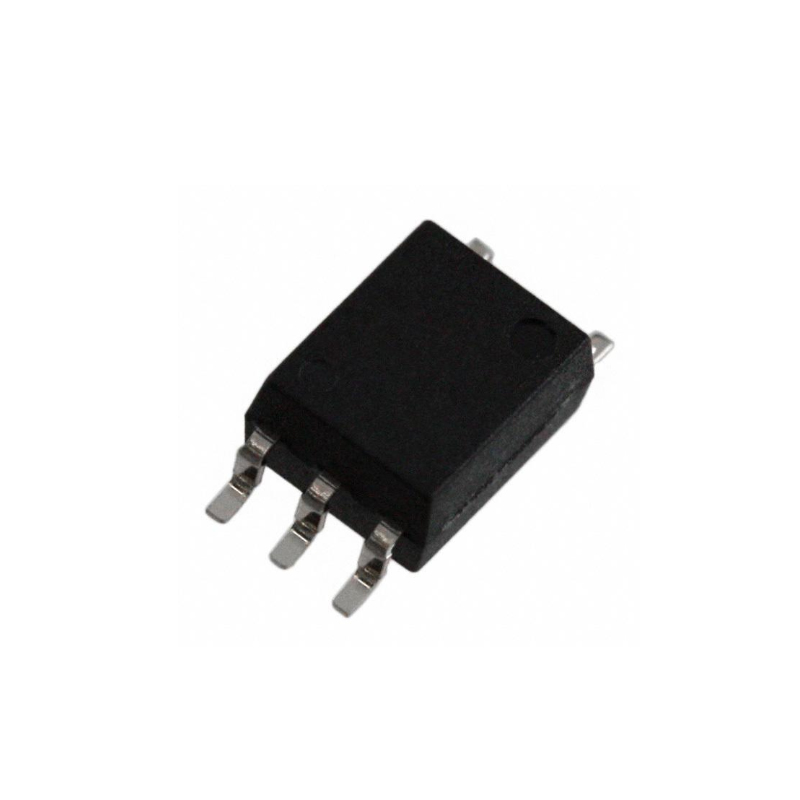
Images are for reference only See Product Specifications
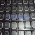
CD4066BM
Four-channel CD4066BM analog switch with a maximum voltage of 20V and an on-state leakage current of 10 picoamps


Brands: Texas Instruments
Mfr.Part #: CD4066BM
Datasheet: CD4066BM Datasheet (PDF)
Package/Case: SOIC (D)-14
RoHS Status:
Stock Condition: 6469 pcs, New Original
Warranty: 1 Year Ovaga Warranty - Find Out More
0
1
Add To BomCD4066BM General Description
The CD4066B device is a quad bilateral switch intended for the transmission or multiplexing of analog or digital signals. It is pin-for-pin compatible with the CD4016B device, but exhibits a much lower on-state resistance. In addition, the on-state resistance is relatively constant over the full signal-input range.
The CD4066B device consists of four bilateral switches, each with independent controls. Both the p and the n devices in a given switch are biased on or off simultaneously by the control signal. As shown in Figure 17, the well of the n-channel device on each switch is tied to either the input (when the switch is on) or to VSS (when the switch is off). This configuration eliminates the variation of the switch-transistor threshold voltage with input signal and, thus, keeps the on-state resistance low over the full operating-signal range.
The advantages over single-channel switches include peak input-signal voltage swings equal to the full supply voltage and more constant on-state impedance over the input-signal range. However, for sample-and-hold applications, the CD4016B device is recommended.
Features
- 15-V Digital or ±7.5-V Peak-to-Peak Switching
- 125-Ω Typical On-State Resistance for
15-V Operation - Switch On-State Resistance Matched to Within
5 Ω Over 15-V Signal-Input Range - On-State Resistance Flat Over Full
Peak-to-Peak Signal Range - High On or Off Output-Voltage Ratio:
80 dB Typical at fis = 10 kHz, RL = 1 kΩ - High Degree of Linearity: <0.5% Distortion Typical at fis = 1 kHz, Vis = 5-Vp-p
VDD – VSS ≥ 10-V, RL = 10 kΩ - Extremely Low Off-State Switch Leakage, Resulting in Very Low Offset Current and High Effective Off-State Resistance: 10 pA Typical at VDD – VSS = 10-V, TA = 25°C
- Extremely High Control Input Impedance
(Control Circuit Isolated From Signal Circuit):
1012 Ω Typical - Low Crosstalk Between Switches: –50 dB Typical at fis = 8 MHz, RL = 1 kΩ
- Matched Control-Input to Signal-Output Capacitance: Reduces Output Signal Transients
- Frequency Response,
Switch On = 40 MHz Typical - 100% Tested for Quiescent Current at 20-V
- 5-V, 10-V, and 15-V Parametric Ratings
Application
Specifications
| Parameter | Value | Parameter | Value |
|---|---|---|---|
| Configuration | 1:1 SPST | Number of channels | 4 |
| Power supply voltage - single (V) | 3.3, 5, 12, 16, 20 | Power supply voltage - dual (V) | +/-10, +/-2.5, +/-5 |
| Protocols | Analog | Ron (typ) (Ω) | 125 |
| CON (typ) (pF) | 8 | Supply current (typ) (µA) | 0.01 |
| Bandwidth (MHz) | 40 | Operating temperature range (°C) | -55 to 125 |
| Input/output continuous current (max) (mA) | 10 | Rating | Catalog |
| Drain supply voltage (max) (V) | 18 | Supply voltage (max) (V) | 18 |
| Negative rail supply voltage (max) (V) | 0 |
Shipping
| Shipping Type | Ship Fee | Lead Time | |
|---|---|---|---|
 |
DHL | $20.00-$40.00 (0.50 KG) | 2-5 days |
 |
Fedex | $20.00-$40.00 (0.50 KG) | 2-5 days |
 |
UPS | $20.00-$40.00 (0.50 KG) | 2-5 days |
 |
TNT | $20.00-$40.00 (0.50 KG) | 2-5 days |
 |
EMS | $20.00-$40.00 (0.50 KG) | 2-5 days |
 |
REGISTERED AIR MAIL | $20.00-$40.00 (0.50 KG) | 2-5 days |
Processing Time:Shipping fee depend on different zone and country.
Payment
| Terms of payment | Hand Fee | |
|---|---|---|
 |
Wire Transfer | charge US$30.00 banking fee. |
 |
Paypal | charge 4.0% service fee. |
 |
Credit Card | charge 3.5% service fee. |
 |
Western Union | charge US.00 banking fee. |
 |
Money Gram | charge US$0.00 banking fee. |
Guarantees
1.The electronic components you purchase include 365 Days Warranty, We guarantee product quality.
2.If some of the items you received aren't of perfect quality, we would resiponsibly arrange your refund or replacement. But the items must remain their orginal condition.
Packing
-

Step1 :Product
-

Step2 :Vacuum packaging
-

Step3 :Anti-static bag
-

Step4 :Individual packaging
-

Step5 :Packaging boxes
-

Step6 :bar-code shipping tag


All the products will packing in anti-staticbag. Ship with ESD antistatic protection.
Outside ESD packing’s lable will use ourcompany’s information: Part Mumber, Brand and Quantity.
We will inspect all the goods before shipment,ensure all the products at good condition and ensure the parts are new originalmatch datasheet.
After all the goods are ensure no problems afterpacking, we will packing safely and send by global express. It exhibitsexcellent puncture and tear resistance along with good seal integrity.


We provide high quality products, thoughtful service and after sale guarantee
-

We have rich products, can meet your various needs.
-

Minimum order quantity starts from 1pcs.
-

Lowest international shipping fee starts from $0.00
-

365 days quality guarantee for all products