Images are for reference only See Product Specifications
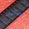
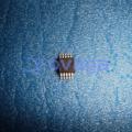
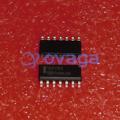
CD4021BE
CMOS 8-Stage Static Shift Register


Brands: Texas Instruments
Mfr.Part #: CD4021BE
Datasheet: CD4021BE Datasheet (PDF)
Package/Case: PDIP (N)-16
RoHS Status:
Stock Condition: 5686 pcs, New Original
Warranty: 1 Year Ovaga Warranty - Find Out More
0
1
Add To BomCD4021BE General Description
CD4014B and CD4021B series types are 8-stage parallel- or serial-input/serial output registers having common CLOCK and PARALLEL/SERIAL CONTROL inputs, a single SERIAL data input, and individual parallel "JAM" inputs to each register stage. Each register stage is D-type, master-slave flip-flop. In addition to an output form stage 8, "Q" outputs are also available from stages 6 and 7. Parallel as well as serial entry is made into the register synchronously with the positive clock line transition in the CD4014B. In the CD4021B serial entry is synchronous with the clock by parallel entry is asynchronous. In both types, entry is controlled by the PARALLEL/SERIAL CONTROL input. When the PARALLEL/SERIAL CONTROL input is low, data is serially shifted into the 8-stage register synchronously with the positive transition of the clock line. When the PARALLEL/SERIAL CONTROL input is high, data is jammed into the 8-stage register via the parallel input lines and synchronous with the positive transition of the clock line. In the CD4021B, the CLOCK input of the internal stage is "forced" when asynchronous parallel entry is made. Register expansion using multiple packages is permitted.
The CD4014B and CD4021B series types are supplied in 16-lead hermetic dual-in-line ceramic packages (F3A suffix), 16-lead dual-in-line plastic packages (E suffix), 16-lead small-outline packages (M, M96, MT, and NSR suffixes), and 16-lead thin shrink small-oultine packages (PW and PWR suffixes).
Features
- Medium speed operation…12 MHz (typ.) clock rate at VDD – VSS = 10 V
- Fully static operation
- 8 master-slave flip-flops plus output buffering and control gating
- 100% tested for quiescent current at 20 V
- Maximum input current of 1 µA at 18 V over full package-temperature range; 100 nA at 18 V and 25°C
- Noise margin (full package-temperature range) =
1 V at VDD = 5 V
2 V at VDD = 10 V
2.5 V at VDD = 15 V - Standardized, symmetrical output characteristics
- 5-V, 10-V, and 15-V parametric ratings
- Meets all requirements of JEDEC Tentative Standard No. 13B, "Standard Specifications for Description of ’B’ Series CMOS Devices"
- Applications:
- Parallel input/serial output data queueing
- Parallel to serial data conversion
- General-purpose register
Data sheet acquired from Harris Semiconductor
Specifications
| Parameter | Value | Parameter | Value |
|---|---|---|---|
| Configuration | Universal | Bits (#) | 8 |
| Technology family | CD4000 | Supply voltage (min) (V) | 3 |
| Supply voltage (max) (V) | 18 | Input type | Standard CMOS |
| Output type | Push-Pull | Clock frequency (MHz) | 8.5 |
| IOL (max) (mA) | 4.2 | IOH (max) (mA) | -4.2 |
| Supply current (max) (µA) | 3000 | Features | Balanced outputs, Positive input clamp diode, Standard speed (tpd > 50ns) |
| Operating temperature range (°C) | -55 to 125 |
Shipping
| Shipping Type | Ship Fee | Lead Time | |
|---|---|---|---|
 |
DHL | $20.00-$40.00 (0.50 KG) | 2-5 days |
 |
Fedex | $20.00-$40.00 (0.50 KG) | 2-5 days |
 |
UPS | $20.00-$40.00 (0.50 KG) | 2-5 days |
 |
TNT | $20.00-$40.00 (0.50 KG) | 2-5 days |
 |
EMS | $20.00-$40.00 (0.50 KG) | 2-5 days |
 |
REGISTERED AIR MAIL | $20.00-$40.00 (0.50 KG) | 2-5 days |
Processing Time:Shipping fee depend on different zone and country.
Payment
| Terms of payment | Hand Fee | |
|---|---|---|
 |
Wire Transfer | charge US$30.00 banking fee. |
 |
Paypal | charge 4.0% service fee. |
 |
Credit Card | charge 3.5% service fee. |
 |
Western Union | charge US.00 banking fee. |
 |
Money Gram | charge US$0.00 banking fee. |
Guarantees
1.The electronic components you purchase include 365 Days Warranty, We guarantee product quality.
2.If some of the items you received aren't of perfect quality, we would resiponsibly arrange your refund or replacement. But the items must remain their orginal condition.
Packing
-

Step1 :Product
-

Step2 :Vacuum packaging
-

Step3 :Anti-static bag
-

Step4 :Individual packaging
-

Step5 :Packaging boxes
-

Step6 :bar-code shipping tag


All the products will packing in anti-staticbag. Ship with ESD antistatic protection.
Outside ESD packing’s lable will use ourcompany’s information: Part Mumber, Brand and Quantity.
We will inspect all the goods before shipment,ensure all the products at good condition and ensure the parts are new originalmatch datasheet.
After all the goods are ensure no problems afterpacking, we will packing safely and send by global express. It exhibitsexcellent puncture and tear resistance along with good seal integrity.


We provide high quality products, thoughtful service and after sale guarantee
-

We have rich products, can meet your various needs.
-

Minimum order quantity starts from 1pcs.
-

Lowest international shipping fee starts from $0.00
-

365 days quality guarantee for all products