Images are for reference only See Product Specifications
Renesas 9FGV0841AKLFT

Clock Generators & Support Products PCIE LOW POWER LOW VOLTAGE


Brands: Renesas Technology Corp
Mfr.Part #: 9FGV0841AKLFT
Datasheet: 9FGV0841AKLFT Datasheet (PDF)
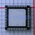
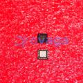
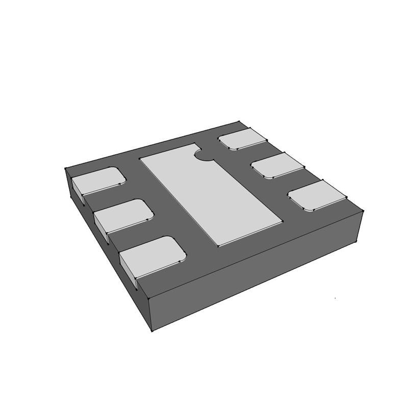
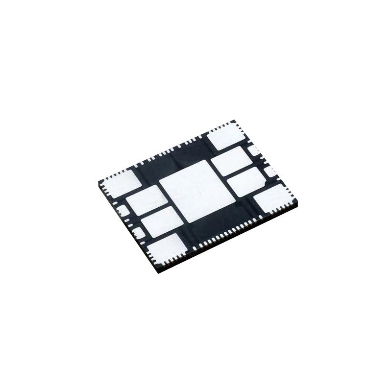
Package/Case: 48-VFQFN
RoHS Status:
Stock Condition: 3475 pcs, New Original
Product Type: Clock & Timer ICs
Warranty: 1 Year Ovaga Warranty - Find Out More
0
1
*All prices are in USD
| Qty | Unit Price | Ext Price |
|---|---|---|
| 1 | $3.410 | $3.410 |
| 200 | $1.321 | $264.200 |
| 500 | $1.274 | $637.000 |
| 1000 | $1.251 | $1251.000 |
In Stock:3475 PCS
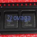
9FGV0841AKLFT General Description
The 9FGV0841 is an 8-output very low power clock generator for PCIe Gen1–4 applications with integrated output terminations providing Zo=100 Ω. The device has 8 output enables for clock management and supports 2 different spread spectrum levels in addition to spread off.
For information regarding evaluation boards and material, please contact your local IDT sales representative.
Features
- PCIe Gen1–4 compliant
- Integrated terminations provide 100Ω differential Zo: reduced component count and board space
- 1.8V operation: reduced power consumption
- Outputs can optionally be supplied from any voltage between 1.05V and 1.8V: maximum power savings
- OE# pins: support DIF power management
- LP-HCSL differential clock outputs: reduced power and board space
- Programmable slew rate for each output: allows tuning for various line lengths
- Programmable output amplitude: allows tuning for various application environments
- DIF outputs blocked until PLL is locked: clean system start-up
- Selectable 0%, -0.25% or -0.5% spread on DIF outputs: reduces EMI
- External 25MHz crystal; supports tight ppm with 0ppm synthesis error
- Configuration can be accomplished with strapping pins: SMBus interface not required for device control
- 3.3V tolerant SMBus interface works with legacy controllers
- Space-saving 6 × 6 mm 48-VFQFPN; minimal board space
- Selectable SMBus addresses: multiple devices can easily share an SMBus segment
- Available in AEC-Q100 qualified, Grade 2 (-40°C to +105°C) version (wettable flank package)
Specifications
| Parameter | Value | Parameter | Value |
|---|---|---|---|
| Pkg. Type | VFQFPN | Lead Count (#) | 48 |
| Temp. Grade | C | Pb (Lead) Free | Yes |
| Carrier Type | Reel |
Shipping
| Shipping Type | Ship Fee | Lead Time | |
|---|---|---|---|
 |
DHL | $20.00-$40.00 (0.50 KG) | 2-5 days |
 |
Fedex | $20.00-$40.00 (0.50 KG) | 2-5 days |
 |
UPS | $20.00-$40.00 (0.50 KG) | 2-5 days |
 |
TNT | $20.00-$40.00 (0.50 KG) | 2-5 days |
 |
EMS | $20.00-$40.00 (0.50 KG) | 2-5 days |
 |
REGISTERED AIR MAIL | $20.00-$40.00 (0.50 KG) | 2-5 days |
Processing Time:Shipping fee depend on different zone and country.
Payment
| Terms of payment | Hand Fee | |
|---|---|---|
 |
Wire Transfer | charge US$30.00 banking fee. |
 |
Paypal | charge 4.0% service fee. |
 |
Credit Card | charge 3.5% service fee. |
 |
Western Union | charge US.00 banking fee. |
 |
Money Gram | charge US$0.00 banking fee. |
Guarantees
1.The electronic components you purchase include 365 Days Warranty, We guarantee product quality.
2.If some of the items you received aren't of perfect quality, we would resiponsibly arrange your refund or replacement. But the items must remain their orginal condition.
Packing
-

Step1 :Product
-

Step2 :Vacuum packaging
-

Step3 :Anti-static bag
-

Step4 :Individual packaging
-

Step5 :Packaging boxes
-

Step6 :bar-code shipping tag


All the products will packing in anti-staticbag. Ship with ESD antistatic protection.
Outside ESD packing’s lable will use ourcompany’s information: Part Mumber, Brand and Quantity.
We will inspect all the goods before shipment,ensure all the products at good condition and ensure the parts are new originalmatch datasheet.
After all the goods are ensure no problems afterpacking, we will packing safely and send by global express. It exhibitsexcellent puncture and tear resistance along with good seal integrity.


Part points
-
The 9FGV0841AKLFT chip is a high-speed differential clock buffer designed for clock distribution and fanout applications in various electronic systems. It offers low additive phase noise, low skew, and low jitter output signals, making it suitable for high-performance applications requiring precise clock synchronization. With its compact size and advanced features, this chip provides an effective solution for clock distribution needs in modern electronic devices.
-
Pinout
The 9FGV0841AKLFT is a quad bidirectional 2:1 multiplexer/demultiplexer with integrated termination resistors. It has a pin count of 24, and its main function is to select one of two data inputs and direct it to the common output line, or to route the input signal to one of the two outputs based on the multiplexing control signal. -
Manufacturer
The manufacturer of the 9FGV0841AKLFT is Intel Corporation. Intel Corporation is an American multinational semiconductor chip manufacturer. -
Application Field
The 9FGV0841AKLFT is a low-power variable gain amplifier (VGA) that is commonly used in wireless communication systems, such as cellular base stations, wireless local area networks (WLANs), and other RF applications. It provides adjustable gain control and helps optimize signal strength and quality in these systems. -
Package
The 9FGV0841AKLFT chip is a 100-pin plastic BGA (ball grid array) package.
Datasheet PDF
We provide high quality products, thoughtful service and after sale guarantee
-

We have rich products, can meet your various needs.
-

Minimum order quantity starts from 1pcs.
-

Lowest international shipping fee starts from $0.00
-

365 days quality guarantee for all products