Simple LED Oscilloscope Circuit Sharing
Update Time: May 12, 2019 Readership: 2823
Contents
The simple LED oscilloscope circuit presented in this article can be used to analyze low frequency waveforms through a 10 x 10 LED matrix display.
Due to the low resolution with only 100 LEDs involved in the display board, the clarity of the waveform display is not that impressive. However, this LED oscilloscope circuit performs quite well in analyzing basic low-frequency waveforms.
Circuit Description
At the heart of the circuit are two ICs, IC2 and IC3, IC LM3915 and IC 4017, respectively.
Before describing the proposed LED oscilloscope circuit in detail, it is important to first understand the brief functional details of these two ICs.
LM3915 Operating Principle
The LM3915 is a dot/bar display driver IC.
The output of this IC is activated sequentially from pin #1 to pin #10 in response to its pin #5 and the increasing voltage level on the ground.
Thus, when a rising potential is applied at pin #5, the low logic is correspondingly shifted from pin #1 to pin #10 in response to this rising potential.
If LEDs are connected to pin #1 and pin #10 with their common anode connected to the positive terminal, these LEDs will light up sequentially from pin #1 up to pin #10 and vice versa in response to the rising and falling voltages on pin #5 and the IC ground.
When IC pin #9 is not connected, all output sequences are unlatched, creating a dot shift for the connected LEDs.
However, when pin #9 is connected to positive power, the output pins of the IC are sequenced in latch mode so that the pin arrangement advances sequentially and latches one after the other, creating a rising bar-like effect on the connected LEDs.
In this LED oscilloscope circuit, IC LM3915 is configured to detect the rising/falling amplitude voltage of the input waveform signal to produce a corresponding shift output in the form of low logic that moves up and down on the LED matrix.
IC 4017 Function
Technically, the IC 4017 is a Johnson decimal counter with 10 decoded outputs.
Like the IC LM3915, the IC 4017 exhibits sequential activation of the outputs from pin #3 to pin #11, however, this sequential shift of the outputs responds to the on/off pulses on its pin #14.
This means that the logic high output shifts from pin #3 to pin #2 when the first positive pulse reaches pin #14, and the logic high pulse shifts from pin #2 to pin #4. when the second pulse reaches pin #14. The sequential shift of the logic high level continues until it reaches pin #11, and when the IC resets, the logic high level returns to pin #3 for a new cycle.
In this LED oscilloscope article, IC 4017 is configured to generate a time base generator that corresponds to the period of the input waveform to be analyzed.
How the LED Oscilloscope Works
The complete circuit schematic of a simple LED oscilloscope is shown in the following figure.
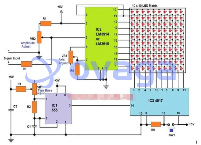
Parts List
- R1 = 150 ohms
- R2, R5 = 1k.
- R3, R6 = 10k
- R4 = 18k
- VR1 = 470k Potentiometer
- VR2 = 4k7 Potentiometer
- VR3 = 2k2 potentiometer
- C1 = 47 nF
- C2 = 10 nF
- SW1 = push-on switch (microswitch)
- IC1 = Any 555 IC
- IC2 = LM3915 or LM3914
- IC3 = Any 4017 IC
- All LEDs are 5 mm red or green, 20 mA type
As described above, IC LM3915 detects the oscillation voltage of the waveform and accordingly generates low logic at its output, which shifts up/down in sequence according to the waveform amplitude.
This upward/downward shift occurs on the Y-axis.
However, in order to track the waveform, we need to make that amplitude sweep across the X-axis so that the waveform is visible on the LED matrix.
This process is done by the IC 4017 output.
Since the IC 4017 output produces a shift logic high and the IC LM3915 output produces a shift logic low, all the anodes of the LEDs are connected to the IC 4017 output and all the cathodes of the LEDs are connected to the IC LM3915 output.
This makes the output of IC 4017 work like a time base generator and the output of IC LM3915 work like a signal modulator.
IC 4017 can also be thought of as a carrier signal generator, just like we have in the AM/FM transmitter waveform.
Now, as mentioned before, the output of IC 4017 will only move sequentially in response to an oscillating pulse applied to its pin #14.
This is achieved with the IC 555 circuit configured as a non-stationary multi-harmonic oscillator.
The oscillation pulses generated at IC 555 pin #3 are applied to IC 4017 pin #14, which causes the output of IC 4017 to generate sequential running high logic from its pin #3 to its pin #11.
How to Generate Waveform Patterns on the LED Matrix
Now, let's analyze what happens when an external waveform signal is applied to pin #5 of IC LM3915.
The LEDs on the Y-axis are controlled by the LM3915 output, which indicates the amplitude of the waveform.
The LED on the X-axis is controlled by the output of IC 4017, which indicates the oscilloscope's time base frequency.
IC LM3915 detects the amplitude of the waveform and generates the corresponding up and down shift low logic on the connected LEDs.
Since 4017 also provides shift logic with a certain frequency, the LM3915 output sweeps the up/down LED illumination on the Y-axis across the X-axis, so it corresponds to the time period of the waveform.
This allows for a simulated sweep waveform pattern on a 10 x 10 LED matrix.
The offset speed of the IC 4017 output determines the direction of the waveform.
If the speed is less than the time period of the waveform, the LED waveform appears to move from right to left, and when the speed is higher than the time period of the waveform, the LED waveform appears to move from left to right.
This speed determines the time base frequency of IC 4017, which is generated by IC 555 non-stationary and can be adjusted with the help of VR1 variable resistor.
Oscilloscope Adjustment
All oscilloscopes are adjusted via potentiometers for three basic adjustments, time base frequency adjustment, amplitude or voltage scale adjustment, and Y-axis position adjustment.
These adjustments allow for proper optimization of the waveform pattern on the screen for proper waveform analysis.
The LED oscilloscope circuit discussed also includes these three basic adjustment functions.
Potentiometer VR1 allows the time base frequency to be adjusted at the IC 4017 output.
Potentiometer VR2 adjusts the voltage level of the waveform on LM3915 pin #5, thus helping to adjust the amplitude voltage scale of the waveform on the LED display.
VR3 helps adjust the Y-axis offset on the 10 x 10 LED matrix display.
Pressing switch SW1 temporarily disables the IC 4017 time base, preventing the waveform from scanning horizontally.
If you have any questions or suggestions about the circuit, feel free to express them via comments.
Popular Blogs
-

Creating a Superior ...
In today's world, technology has become an essen...
-

How the Integrated D...
In order to improve efficiency without affecting...
-
Simple LED Oscillosc...
The simple LED oscilloscope circuit presented in...
-
Could Super-surfaces...
A major focus of technological advances in many ...
Hot Products

Popular Manufacturers